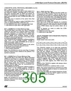
J1850 Byte Level Protocol Decoder (JBLPD)
J1850 BYTE LEVEL PROTOCOL DECODER (Cont’d)
10.9.6.4 DMA Management in Transmission
Mode
Register pair); it is the next location in the TX-
DATA transfer cycle;
DMA in transmission is performed when the TRDY
bit of the STATUS register is set (by hardware).
The TRDY bit is reset as soon as the DMA cycle is
finished.
To enable the DMA feature, the TXD_M bit in the
IMR register must be set (by software).
– A post-increment of the DMA Address Register
(or Register pair);
– A post-decrement of the DMA transaction coun-
ter, which contains the number of transactions
that have still to be performed.
Note: When the TEOBP pending bit is set (at the
end of the last DMA transfer), the transmission
DMA enable bit (TXD_M) is automatically reset by
hardware. However, the DMA can be disabled by
software resetting the TXD_M bit.
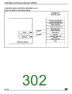
Compared to reception, in transmission each DMA
request performs the transfer of either a single
byte or a couple of bytes depending on the value
of the Transmit Opcode bits (TXOP.OP[2:0]) writ-
ten during the DMA transfer.
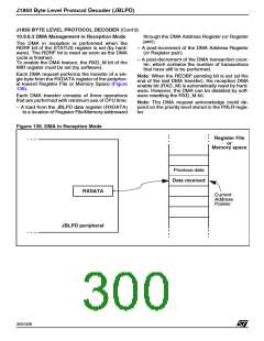
The table of values managed by the DMA must be
a sequence of opcode bytes (that will be written in
the TXOP register by the DMA) each one followed
by a data byte (that will be written in the TXDATA
register by the DMA) if the opcode needs it (see
Figure 140).
Note: When using DMA, the TXOP byte is written
before the TXDATA register. This order is accept-
ed by the JBLPD only when the DMA in transmis-
sion is enabled.
Note: The DMA request acknowledge could de-
pend on the priority level stored in the PRLR regis-
ter. In the same way, some time can occur be-
tween the transfer of the first byte and the transfer
of the second one if another interrupt or DMA re-
quest with higher priority occurs.
Each DMA cycle consists of the following transfers
for a total of three/six operations that are per-
formed with minimum use of CPU time:
– A load to the JBLPD Transmit Opcode register
(TXOP) from a location of Register File/Memory
addressed through the DMA Address Register
(or Register pair);
10.9.6.5 DMA Suspend mode
In the JBLPD it is possible to suspend or not to
suspend the DMA transfer while some J1850 pro-
tocol events occur. The selection between the two
modes is done by programming the DMASUSP bit
of the OPTIONS register.
If the DMASUSP bit is set (DMA suspended
mode), while the ERROR or TLA flag is set, the
DMA transfers are suspended, to allow the user
program to handle the event condition.
– A post-increment of the DMA Address Register
(or Register pair);
– A post-decrement of the DMA transaction coun-
ter, which contains the number of transactions
that have still to be performed;
and if the Transmit Opcode placed in TXOP re-
quires a datum:
– A load to the peripheral data register (TXDATA)
from a location of Register File/Memory ad-
dressed through the DMA Address Register (or
If the DMASUSP bit is reset (DMA not suspended
mode), the previous flags have no effect on the
DMA transfers.
301/426
9

 STMICROELECTRONICS [ ST ]