J1850 Byte Level Protocol Decoder (JBLPD)
J1850 BYTE LEVEL PROTOCOL DECODER (Cont’d)
Transmit Opcode Queuing
JBLPD has a receiver pin which tells the transmit-
ter about bus activity. Due to characteristics of the
J1850 bus and the eight-clock digital filter, the sig-
nals presented to the VPW symbol decoder are
delayed a certain amount of time behind the actual
J1850 bus. Also, due to wave shaping and other
signal conditioning of the transceiver I.C. the ac-
tions of the VPWO pin on the transmitter take time
to appear on the bus itself. The total external
J1850 bus delays are defined in the SAE J1850
standard as nominally 16 µs. The nominal 16 µs
loop delay will actually vary between different
transceiver I.C’s. The JBLPD peripheral thus in-
cludes a programmability of the external loop de-
lay in the bit positions JDLY[4:0]. This assures
only nominal transmit symbols are placed on the
bus by the JBLPD.
The JBLPD has the capability of queuing opcode
transmits written to the TXOP register until J1850
bus conditions are in a correct state for the trans-
mit to occur. For example, a MSGx opcode can be
queued when the JBLPD is presently receiving a
frame (or transmitting a MSG+CRC opcode) or an
IFRx opcode can be queued when currently re-
ceiving or transmitting the message portion of a
frame.
Queuing a MSG or MSG+CRC opcode for the next
frame can occur while another frame is in
progress. A MSGx opcode is written to the TXOP
register when the present frame is past the point
where arbitration for control of the bus for this
frame can occur. The JBLPD will wait for a nomi-
nal IFS symbol (or EOFmin if another node begins
early) to appear on the VPWI line before com-
mencing to transmit this queued opcode. The
TRDY bit for the queued opcode will remain clear
until the EOFmin is detected on the VPWI line
where it will then get set. Queued MSGx transmits
for the next frame do not get cancelled for TLA,
IBD, IFD or CRCE errors that occur in the present
frame. An RBRK error will cancel a queued op-
code for the next frame.
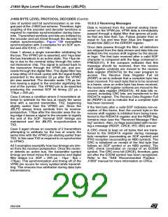
The method of transmitting for the JBLPD includes
interaction between the transmitter and the receiv-
er. The transmitter starts a symbol by placing the
proper level (active or passive) on its VPWO pin.
The transmitter then waits for the corresponding
pin transition (inverted, of course) at the VPW de-
coder input. Note that the level may actually ap-
pear at the input before the transmitter places the
value on the VPWO pin. Timing of the remainder
of the symbol starts when the transition is detect-
ed. Refer to Figure 136, Case 1. The symbol time-
out value is defined as:
Queuing an IFRx opcode for the present frame
can occur at any time after the detection of the be-
ginning of an SOF character from the VPWI line.
The queued IFR will wait for a nominal EOD sym-
bol (or EODmin if another node begins early) be-
fore commencing to transmit the IFR. A queued
IFR transmit will be cancelled on IBD, lFD, CRCE,
RBRK errors as well as on a correct message
length check error or frame length limit violation if
these checks are enabled.
SymbolTimeout = NominalSymbolTime - ExternalLoop-
Delay - 8 µs
NominalSymbolTime = Tv Symbol time
ExternalLoopDelay = defined via JDLY[4:0]
8 µs = Digital Filter
Bit-by-bit arbitration must be used to settle the
conflicts that occur when multiple nodes attempt to
transmit frames simultaneously. Arbitration is ap-
plied to each data bit symbol transmitted starting
after the SOF or NBx symbol and continuing until
the EOD symbol. During simultaneous transmis-
sions of active and passive states on the bus, the
resultant state on the bus is the active state. If the
JBLPD detects a received symbol from the bus
that is different from the symbol being transmitted,
then the JBLPD will discontinue its transmit opera-
tion prior to the start of the next bit. Once arbitra-
tion has been lost, the VPWO pin must go passive
within one period of the prescaled clock of the pe-
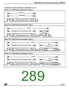
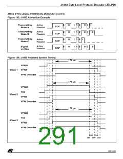
ripheral. Figure 135 shows 3 nodes attempting to
arbitrate for the bus with Node B eventually win-
ning with the highest priority data.
Transmit Bus Timing, Arbitration, and Syn-
chronization
The external J1850 bus on the other side of the
transceiver I.C. is a single wire multiplex bus with
multiple nodes transmitting a number of different
types of message frames. Each node can transmit
at any time and synchronization and arbitration is
used to determine who wins control of the trans-
mit. It is the obligation of the JBLPD transmitter
section to synchronize off of symbols on the bus,
and to place only nominal symbol times onto the
bus within the accuracy of the peripheral (+/- 1 µs).
To transmit proper symbols the JBLPD must know
what is going on out on the bus. Fortunately, the
290/426
9

 STMICROELECTRONICS [ ST ]