I2C BUS INTERFACE
2
I C BUS INTERFACE (Cont’d)
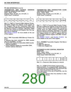
TRANSMITTER DMA SOURCE ADDRESS
POINTER REGISTER (I2CTDAP)
R252 - Read / Write
Register Page: 20 (I2C_0) or 22 (I2C_1)
Reset Value: Undefined
TRANSMITTER DMA TRANSACTION COUN-
TER REGISTER (I2CTDC)
R253 - Read / Write
Register Page: 20 (I2C_0) or 22 (I2C_1)
Reset Value: Undefined
7
0
7
0
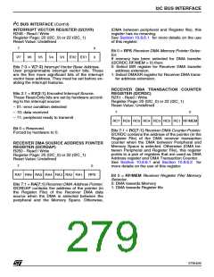
TA7 TA6 TA5 TA4 TA3 TA2 TA1
TPS
TC7 TC6 TC5 TC4 TC3 TC2 TC1 RF/MEM
Bits 7:1= TA[7:1] Transmit DMA Address Pointer.
I2CTDAP contains the address of the pointer (in
the Register File) of the Transmitter DMA data
source when the DMA between the peripheral and
the Memory Space is selected. Otherwise (DMA
between the peripheral and Register file), this reg-
ister has no meaning.
Bits 7:1 = TC[7:1] Transmit DMA Counter Pointer.
I2CTDC contains the address of the pointer (in the
Register File) of the DMA transmitter transaction
counter when the DMA between Peripheral and
Memory Space is selected. Otherwise, if the DMA
between Peripheral and Register File is selected,
this register points to a pair of registers that are
used as DMA Address register and DMA Transac-
tion Counter.
See Section 10.8.6.2 for more details on the use
of this register.
See Section 10.8.6.1 and Section 10.8.6.2 for
more details on the use of this register.
Bit 0 = TPS Transmitter DMA Memory Pointer Se-
lector.
If memory has been selected for DMA transfer
(I2CTDC.RF/MEM = 0) then:
0: Select ISR register for transmitter DMA transfer
address extension.
1: Select DMASR register for transmitter DMA
transfer address extension.
Bit 0 = RF/MEM Transmitter Register File/ Memo-
ry Selector.
0: DMA from Memory
1: DMA from Register file
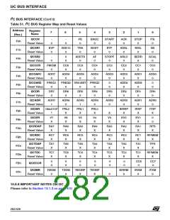
EXTENDED CLOCK CONTROL REGISTER
(I2CECCR)
R254 - Read / Write
Register Page: 20 (I2C_0) or 22 (I2C_1)
Reset Value: 0000 0000 (00h)
7
0
0
0
0
0
0
0
CC8 CC7
Bits 7:2 = Reserved. Must always be cleared.
Bits 1:0 = CC[8:7] 9-bit divider programming
Implementation of a programmable clock divider.
These bits and the CC[6:0] bits of the I2CCCR reg-
ister select the speed of the bus (F
).
SCL
For a description of the use of these bits, see the
I2CCCR register.
They are not cleared when the interface is disa-
bled (I2CCCR.PE=0).
280/426
9

 STMICROELECTRONICS [ ST ]