I2C BUS INTERFACE
2
I C BUS INTERFACE (Cont’d)
2
2
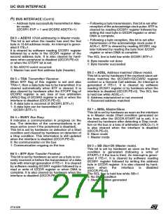
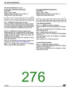
I C CLOCK CONTROL REGISTER
(I2CCCR)
I C OWN ADDRESS REGISTER 1
(I2COAR1)
R243 - Read / Write
Register Page: 20 (I2C_0) or 22 (I2C_1)
Reset Value: 0000 0000 (00h)
R244 - Read / Write
Register Page: 20 (I2C_0) or 22 (I2C_1)
Reset Value: 0000 0000 (00h)
7
0
7
0
FM/SM CC6 CC5 CC4 CC3 CC2 CC1 CC0
ADD7 ADD6 ADD5 ADD4 ADD3 ADD2 ADD1 ADD0
2
Bit 7 = FM/SM Fast/Standard I C mode.
7-bit Addressing Mode
This bit is used to select between fast and stand-
ard mode. See the description of the following bits.
It is set and cleared by software. It is not cleared
when the peripheral is disabled (I2CCR.PE=0)
Bits 7:1 = ADD[7:1] Interface address.
2
These bits define the I C bus address of the inter-
face.
They are not cleared when the interface is disa-
bled (I2CCR.PE=0).
Bits 6:0 = CC[6:0] 9-bit divider programming
Implementation of a programmable clock divider.
These bits and the CC[8:7] bits of the I2CECCR
Bit 0 = ADD0 Address direction bit.
This bit is don’t care; the interface acknowledges
either 0 or 1.
It is not cleared when the interface is disabled
(I2CCR.PE=0).
register select the speed of the bus (F
) de-
SCL
2
pending on the I C mode.
They are not cleared when the interface is disa-
bled (I2CCR.PE=0).
Note: Address 01h is always ignored.
Refer to the Electrical Characteristics section for
the table of values (Table 70 on page 398).
10-bit Addressing Mode
Note: The programmed frequency is available
with no load on SCL and SDA pins.
Bits 7:0 = ADD[7:0] Interface address.
2
These are the least significant bits of the I Cbus
address of the interface.
They are not cleared when the interface is disa-
bled (I2CCR.PE=0).
276/426
9

 STMICROELECTRONICS [ ST ]