I2C BUS INTERFACE
2
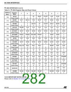
I C BUS INTERFACE (Cont’d)
INTERRUPT STATUS REGISTER (I2CISR)
R248 - Read / Write
Register Page: 20 (I2C_0) or 22 (I2C_1)
Reset Value: 1xxx xxxx (xxh)
Note: The Interrupt pending bits can be reset by
writing a “0” but is not possible to write a “1”. It is
mandatory to clear the interrupt source by writing a
“0” in the pending bit when executing the interrupt
service routine. When serving an interrupt routine,
the user should reset ONLY the pending bit related
to the served interrupt routine (and not reset the
other pending bits).
7
0
1
PRL2 PRL1 PRL0
0
IERRP IRXP ITXP
To detect the specific error condition that oc-
curred, the flag bits of the I2CSR1 and I2CSR2
register should be checked.
Bit 7 = Reserved.
Must be kept at 1
Note: The IERRP pending bit is forced high when-
the error event flags are set (ADSL and SB flags in
the I2CSR1 register, SCLF, ADDTX, AF, STOPF,
ARLO and BERR flags in the I2CSR2 register). If
at least one flag is set, the application code should
not reset the IERRP bit.
Bits 6:4 = PRL[2:0] Interrupt/DMA Priority Bits.
The priority is encoded with these three bits. The
value of “0” has the highest priority, the value “7”
has no priority. After the setting of this priority lev-
el, the priorities between the different Interrupt/
DMA sources is hardware defined according with
the following scheme:
Bit 1 = IRXP Data Received pending bit
0: No data received
1: data received (if ITE=1).
– Error condition Interrupt (If DMASTOP=1) (High-
est priority)
– Receiver DMA request
Bit 0 = ITXP Peripheral Ready To Transmit pend-
– Transmitter DMA request
ing bit
– Error Condition Interrupt (If DMASTOP=0
– Data Received/Receiver End Of Block
0: Peripheral not ready to transmit
1: Peripheral ready to transmit a data byte (if
ITE=1).
– Peripheral Ready To Transmit/Transmitter End
Of Block (Lowest priority)
Bit 3 = Reserved.
Must be cleared.
Bit 2 = IERRP Error Condition pending bit
0: No error
1: Error event detected (if ITE=1)
278/426
9

 STMICROELECTRONICS [ ST ]