I2C BUS INTERFACE
2
I C BUS INTERFACE (Cont’d)
10.8.7 Register Description
1: The General Call address stored in the I2CADR
register will be acknowledged
Note: The correct value (usually 00h) must be
written in the I2CADR register before enabling the
General Call feature.
IMPORTANT:
1. To guarantee correct operation, before enabling
the peripheral (while I2CCR.PE=0), configure bit7
and bit6 of the I2COAR2 register according to the
internal clock INTCLK (for example 11xxxxxxb in
the range 14 - 30 MHz).
Bit 3 = START Generation of a Start condition.
This bit is set and cleared by software. It is also
cleared by hardware when the interface is disa-
bled (I2CCR.PE=0) or when the Start condition is
sent (with interrupt generation if ITE=1).
– In master mode:
2. Bit7 of the I2CCR register must be cleared.
2
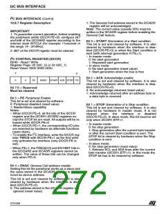
I C CONTROL REGISTER (I2CCR)
0: No start generation
R240 - Read / Write
1: Repeated start generation
Register Page: 20 (I2C_0) or 22 (I2C_1)
Reset Value: 0000 0000 (00h)
– In slave mode:
0: No start generation (reset value)
1: Start generation when the bus is free
7
0
Bit 2 = ACK Acknowledge enable.
0
0
PE
ENGC START ACK STOP ITE
This bit is set and cleared by software. It is also
cleared by hardware when the interface is disa-
bled (I2CCR.PE=0).
Bit 7:6 = Reserved
Must be cleared
0: No acknowledge returned (reset value)
1: Acknowledge returned after an address byte or
a data byte is received
Bit 5 = PE Peripheral Enable.
This bit is set and cleared by software.
0: Peripheral disabled (reset value)
1: Master/Slave capability
Bit 1 = STOP Generation of a Stop condition.
This bit is set and cleared by software. It is also
cleared by hardware in master mode. It is not
cleared when the interface is disabled
(I2CCR.PE=0). In slave mode, this bit must be set
only when I2CSR1.BTF=1.
Notes:
– When I2CCR.PE=0, all the bits of the I2CCR
register and the I2CSR1-I2CSR2 registers ex-
cept the STOP bit are reset. All outputs will be re-
leased while I2CCR.PE=0
– In master mode:
0: No stop generation
1: Stop generation after the current byte transfer
or after the current Start condition is sent. The
STOP bit is cleared by hardware when the Stop
condition is sent.
– When I2CCR.PE=1, the corresponding I/O pins
are selected by hardware as alternate functions
(open drain).
2
– To enable the I C interface, write the I2CCR reg-
ister TWICE with I2CCR.PE=1 as the first write
only activates the interface (only I2CCR.PE is
set).
– In slave mode:
0: No stop generation (reset value)
1: Release SCL and SDA lines after the current
byte transfer (I2CSR1.BTF=1). In this mode the
STOP bit has to be cleared by software.
– When PE=1, the FREQ[2:0] and EN10BIT bits in
the I2COAR2 and I2CADR registers cannot be
written. The value of these bits can be changed
only when PE=0.
Bit 4 = ENGC General Call address enable.
Setting this bit the peripheral works as a slave and
the value stored in the I2CADR register is recog-
nized as device address.
This bit is set and cleared by software. It is also
cleared by hardware when the interface is disa-
bled (I2CCR.PE=0).
0: The address stored in the I2CADR register is
ignored (reset value)
272/426
9

 STMICROELECTRONICS [ ST ]