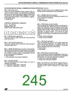
ASYNCHRONOUS SERIAL COMMUNICATIONS INTERFACE (SCI-A)
ASYNCHRONOUS SERIAL COMMUNICATIONS INTERFACE (Cont’d)
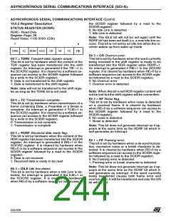
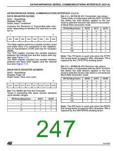
DATA REGISTER (SCIDR)
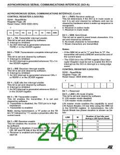
Bits 5:3 = SCT[2:0] SCI Transmitter rate divisor
These 3 bits, in conjunction with the SCP1 & SCP0
bits define the total division applied to the bus
clock to yield the transmit rate clock in convention-
al Baud Rate Generator mode.
R241 - Read/Write
Register Page: 26
Reset Value: Undefined
Contains the Received or Transmitted data char-
acter, depending on whether it is read from or writ-
ten to.
TR Dividing Factor
SCT2
SCT1
SCT0
1
2
0
0
0
0
1
1
1
1
0
0
1
1
0
0
1
1
0
1
0
1
0
1
0
1
7
0
4
DR7
DR6
DR5
DR4
DR3
DR2
DR1
DR0
8
16
32
64
128
The Data register performs a double function (read
and write) since it is composed of two registers,
one for transmission (TDR) and one for reception
(RDR).
The TDR register provides the parallel interface
between the internal bus and the output shift reg-
ister (see Figure 117).
The RDR register provides the parallel interface
between the input shift register and the internal
bus (see Figure 117).
Note: This TR factor is used only when the ETPR
fine tuning factor is equal to 00h; otherwise, TR is
replaced by the (TR*ETPR) dividing factor.
Bits 2:0 = SCR[2:0] SCI Receiver rate divisor.
These 3 bits, in conjunction with the SCP1 & SCP0
bits define the total division applied to the bus
clock to yield the receive rate clock in conventional
Baud Rate Generator mode.
BAUD RATE REGISTER (SCIBRR)
R242 - Read/Write
Register Page: 26
Reset Value: 00xx xxxx (xxh)
RR Dividing Factor
SCR2
SCR1
SCR0
7
0
1
2
0
0
0
0
1
1
1
1
0
0
1
1
0
0
1
1
0
1
0
1
0
1
0
1
SCP1 SCP0 SCT2 SCT1 SCT0 SCR2 SCR1 SCR0
4
8
Bits 7:6= SCP[1:0] First SCI Prescaler
These 2 prescaling bits allow several standard
clock division ranges:
16
32
64
128
PR Prescaling factor
SCP1
SCP0
1
3
0
0
1
1
0
1
0
1
Note: This RR factor is used only when the ERPR
fine tuning factor is equal to 00h; otherwise, RR is
replaced by the (RR*ERPR) dividing factor.
4
13
247/426
9

 STMICROELECTRONICS [ ST ]