ASYNCHRONOUS SERIAL COMMUNICATIONS INTERFACE (SCI-A)
ASYNCHRONOUS SERIAL COMMUNICATIONS INTERFACE (Cont’d)
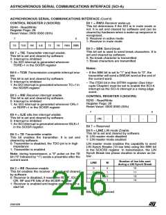
CONTROL REGISTER 2 (SCICR2)
Bit 1 = RWU Receiver wake-up.
This bit determines if the SCI is in mute mode or
not. It is set and cleared by software and can be
cleared by hardware when a wake-up sequence is
recognized.
R244 - Read/Write
Register Page: 26
Reset Value: 0000 0000 (00h)
0: Receiver in active mode
1: Receiver in mute mode
7
0
TIE
TCIE
RIE
ILIE
TE
RE
RWU
SBK
Bit 0 = SBK Send break.
This bit set is used to send break characters. It is
set and cleared by software.
0: No break character is transmitted
1: Break characters are transmitted
Bit 7 = TIE Transmitter interrupt enable.
This bit is set and cleared by software.
0: Interrupt is inhibited
1: An SCI interrupt is generated whenever
TDRE=1 in the SCISR register
Notes:
– If the SBK bit is set to “1” and then to “0”, the
transmitter will send a BREAK word at the end of
the current word.
Bit 6 = TCIE Transmission complete interrupt ena-
ble
This bit is set and cleared by software.
0: Interrupt is inhibited
1: An SCI interrupt is generated whenever TC=1 in
the SCISR register
– The ITEI0 bit in the SITRH register (See Inter-
rupts Chapter) must be set to enable the SCI-A
interrupt as the SCI-A interrupt is a rising edge
event.
Bit 5 = RIE Receiver interrupt enable.
This bit is set and cleared by software.
0: Interrupt is inhibited
1: An SCI interrupt is generated whenever OR=1
or RDRF=1 in the SCISR register
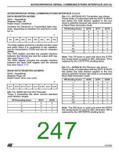
CONTROL REGISTER 3 (SCICR3)
R255 - Read/Write
Register Page: 26
Reset Value: 0000 0000 (00h)
7
0
-
Bit 4 = ILIE Idle line interrupt enable.
This bit is set and cleared by software.
0: Interrupt is inhibited
-
LINE
-
-
-
-
-
1: An SCI interrupt is generated whenever IDLE=1
in the SCISR register.
Bit 7 = Reserved
Bit 6 = LINE LIN mode Enable.
This bit is set and cleared by software.
0: LIN master mode disabled
1: LIN master mode enabled
Bit 3 = TE Transmitter enable.
This bit enables the transmitter. It is set and
cleared by software.
0: Transmitter is disabled, the TDO pin is in high
impedance
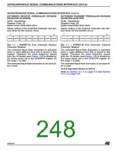
LIN master mode enables the capability to send
LIN Synch Breaks (13 low bits) using the SBK bit
in the SCICR2 register. In transmission, the LIN
Synch Break low phase duration is shown as be-
low:
1: Transmitter is enabled
Note: during transmission, a “0” pulse on the TE
bit (“0” followed by “1”) sends a preamble after the
current word.
Number of low bits sent
LINE
M
during a LIN Synch Break
0
0
1
1
0
1
0
1
10
11
13
14
Bit 2 = RE Receiver enable.
This bit enables the receiver. It is set and cleared
by software.
0: Receiver is disabled, it resets the RDRF, IDLE,
OR, NF and FE bits of the SCISR register
1: Receiver is enabled and begins searching for a
start bit
Bits 5:0 = Reserved
246/426
9

 STMICROELECTRONICS [ ST ]