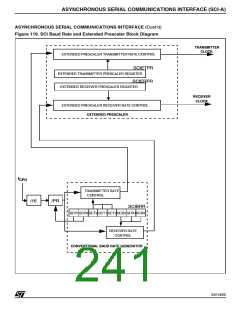
ASYNCHRONOUS SERIAL COMMUNICATIONS INTERFACE (SCI-A)
ASYNCHRONOUS SERIAL COMMUNICATIONS INTERFACE (Cont’d)
Bit 0 = PE Parity error.
Note: The M bit must not be modified during a data
This bit is set by hardware when a parity error oc-
curs in receiver mode. It is cleared by a software
sequence (a read to the status register followed by
an access to the SCIDR data register). An inter-
rupt is generated if PIE=1 in the SCICR1 register.
0: No parity error
transfer (both transmission and reception).
Bit 3 = WAKE Wake-Up method.
This bit determines the SCI Wake-Up method, it is
set or cleared by software.
0: Idle Line
1: Parity error
1: Address Mark
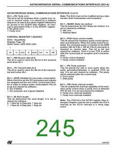
CONTROL REGISTER 1 (SCICR1)
Bit 2 = PCE Parity control enable.
R243 - Read/Write
Register Page: 26
Reset Value: x000 0000 (x0h)
This bit selects the hardware parity control (gener-
ation and detection). When the parity control is en-
abled, the computed parity is inserted at the MSB
position (9th bit if M=1; 8th bit if M=0) and parity is
checked on receive data. This bit is set and
cleared by software. Once it is set, PCE is active
after the current byte (in reception and in transmis-
sion).
7
0
R8
T8
SCID
M
WAKE PCE
PS
PIE
0: Parity control disabled
1: Parity control enabled
Bit 7 = R8 Receive data bit 8.
This bit is used to store the 9th bit of the received
word when M=1.
Bit 1 = PS Parity selection.
This bit selects the odd or even parity when the
parity generation/detection is enabled (PCE bit
set). It is set and cleared by software. The parity
will be selected after the current byte.
0: Even parity
Bit 6 = T8 Transmit data bit 8.
This bit is used to store the 9th bit of the transmit-
ted word when M=1.
Bit 5 = SCID Disabled for low power consumption
When this bit is set the SCI prescalers and outputs
are stopped and the end of the current byte trans-
fer in order to reduce power consumption.This bit
is set and cleared by software.
0: SCI enabled
1: SCI prescaler and outputs disabled
1: Odd parity
Bit 0 = PIE Parity interrupt enable.
This bit enables the interrupt capability of the hard-
ware parity control when a parity error is detected
(PE bit set). It is set and cleared by software.
0: Parity error interrupt disabled
1: Parity error interrupt enabled
Bit 4 = M Word length.
This bit determines the word length. It is set or
cleared by software.
0: 1 Start bit, 8 Data bits, 1 Stop bit
1: 1 Start bit, 9 Data bits, 1 Stop bit
Note: The ITEI0 bit in the SITRH register (See In-
terrupts Chapter) must be set to enable the SCI-A
interrupt as the SCI-A interrupt is a rising edge
event.
245/426
9

 STMICROELECTRONICS [ ST ]