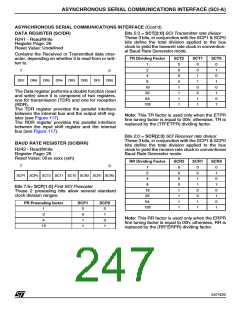
ASYNCHRONOUS SERIAL COMMUNICATIONS INTERFACE (SCI-A)
ASYNCHRONOUS SERIAL COMMUNICATIONS INTERFACE (Cont’d)
10.6.4.7 Parity definition
Transmission mode: If the PCE bit is set then the
MSB bit of the data written in the data register is
not transmitted but is changed by the parity bit.
Even parity: The parity bit is calculated to obtain
an even number of “1s” inside the frame made of
the 7 or 8 LSB bits (depending on whether M is
equal to 0 or 1) and the parity bit.
Reception mode: If the PCE bit is set then the in-
terface checks if the received data byte has an
even number of “1s” if even parity is selected
(PS=0) or an odd number of “1s” if odd parity is se-
lected (PS=1). If the parity check fails, the PE flag
is set in the SCISR register and an interrupt is gen-
erated if PCIE is set in the SCICR1 register.
Ex: data=00110101; 4 bits set => parity bit will be
0 if even parity is selected (PS bit = 0).
Odd parity: The parity bit is calculated to obtain
an odd number of “1s” inside the frame made of
the 7 or 8 LSB bits (depending on whether M is
equal to 0 or 1) and the parity bit.
Ex: data=00110101; 4 bits set => parity bit will be
1 if odd parity is selected (PS bit = 1).
243/426
9

 STMICROELECTRONICS [ ST ]