ASYNCHRONOUS SERIAL COMMUNICATIONS INTERFACE (SCI-A)
ASYNCHRONOUS SERIAL COMMUNICATIONS INTERFACE (Cont’d)
10.6.4.4 Conventional Baud Rate Generation
10.6.4.6 Receiver Muting and Wake-up Feature
The baud rate for the receiver and transmitter (Rx
and Tx) are set independently and calculated as
follows:
In multiprocessor configurations it is often desira-
ble that only the intended message recipient
should actively receive the full message contents,
thus reducing redundant SCI service overhead for
all non addressed receivers.
f
f
CPU
CPU
Rx =
Tx =
The non addressed devices may be placed in
sleep mode by means of the muting function.
(16 PR) RR
(16 PR) TR
*
*
*
*
with:
Setting the RWU bit by software puts the SCI in
sleep mode:
PR = 1, 3, 4 or 13 (see SCP[1:0] bits)
TR = 1, 2, 4, 8, 16, 32, 64,128
(see SCT[2:0] bits)
All the reception status bits can not be set.
All the receive interrupt are inhibited.
RR = 1, 2, 4, 8, 16, 32, 64,128
(see SCR[2:0] bits)
A muted receiver may be awakened by one of the
following two ways:
– by Idle Line detection if the WAKE bit is reset,
– by Address Mark detection if the WAKE bit is set.
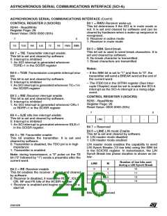
All this bits are in the SCIBRR register.
Example: If f
is 24 MHz and if PR=13 and
TR=RR=2, the transmit and receive baud rates are
57700 baud.
CPU
Receiver wakes-up by Idle Line detection when
the Receive line has recognised an Idle Frame.
Then the RWU bit is reset by hardware but the
IDLE bit is not set.
Note: The baud rate registers MUST NOT be
changed while the transmitter or the receiver is en-
abled.
Receiver wakes-up by Address Mark detection
when it received a “1” as the most significant bit of
a word, thus indicating that the message is an ad-
dress. The reception of this particular word wakes
up the receiver, resets the RWU bit and sets the
RDRF bit, which allows the receiver to receive this
word normally and to use it as an address word.
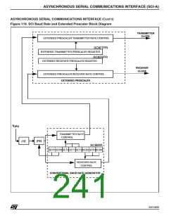
10.6.4.5 Extended Baud Rate Generation
The extended prescaler option gives a very fine
tuning on the baud rate, using a 255 value prescal-
er, whereas the conventional Baud Rate Genera-
tor retains industry standard software compatibili-
ty.
The extended Baud Rate Generator block diagram
is described in the Figure 119.
M Bit
PCE Bit
SCI Frame
0
0
1
1
0
1
0
1
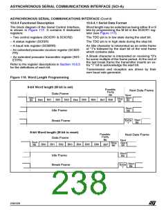
| SB | 8 bit data | STB |
| SB | 7-bit data | PB | STB |
| SB | 9-bit data | STB |
| SB | 8-bit data PB | STB |
The output clock rate sent to the transmitter or to
the receiver will be the output from the 16 divider
divided by a factor ranging from 1 to 255 set in the
SCIERPR or the SCIETPR register.
Note: The extended prescaler is activated by set-
ting the SCIETPR or SCIERPR register to a value
other than zero. The baud rates are calculated as
follows:
SB : Start Bit
STB : Stop Bit
PB : Parity Bit
f
f
CPU
CPU
Rx =
16 ERPR*(PR*TR)
Tx =
16 ETPR*(PR*TR)
Note: In case of wake up by an address mark, the
MSB bit of the data is taken into account and not
the parity bit
*
*
with:
ETPR = 1,..,255 (see SCIETPR register)
ERPR = 1,.. 255 (see SCIERPR register)
242/426
9

 STMICROELECTRONICS [ ST ]