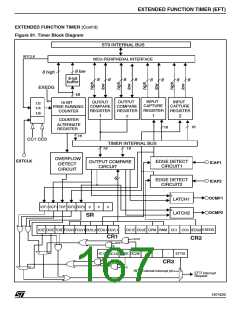
EXTENDED FUNCTION TIMER (EFT)
EXTENDED FUNCTION TIMER (Cont’d)
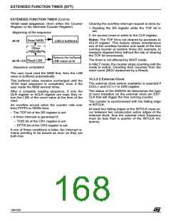
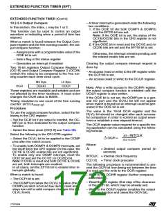
16-bit read sequence: (from either the Counter
Clearing the overflow interrupt request is done by:
Register or the Alternate Counter Register).
1. Reading the SR register while the TOF bit is
set.
Beginning of the sequence
2. An access (read or write) to the CLR register.
Notes: The TOF bit is not cleared by accesses to
ACLR register. This feature allows simultaneous
use of the overflow function and reads of the free
running counter at random times (for example, to
measure elapsed time) without the risk of clearing
the TOF bit erroneously.
Read MSB
At t0
LSB is buffered
Other
instructions
Returns the buffered
LSB value at t0
The timer is not affected by WAIT mode.
Read LSB
At t0 +Dt
In HALT mode, the counter stops counting until the
mode is exited. Counting then resumes from the
reset count (MCU awakened by a Reset).
Sequence completed
The user must read the MSB first, then the LSB
value is buffered automatically.
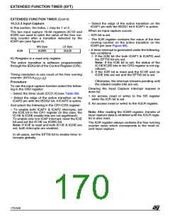
10.3.3.2 External Clock
This buffered value remains unchanged until the
16-bit read sequence is completed, even if the
user reads the MSB several times.
The external clock (where available) is selected if
CC0=1 and CC1=1 in CR2 register.
The status of the EXEDG bit determines the type
of level transition on the external clock pin EXT-
CLK that will trigger the free running counter.
After a complete reading sequence, if only the
CLR register or ACLR register are read, they re-
turn the LSB of the count value at the time of the
read.
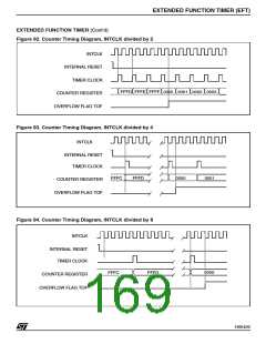
The counter is synchronised with the falling edge
of INTCLK.
An overflow occurs when the counter rolls over
from FFFFh to 0000h then:
At least four falling edges of the INTCLK must oc-
cur between two consecutive active edges of the
external clock; thus the external clock frequency
must be less than a quarter of the INTCLK fre-
quency.
– The TOF bit of the SR register is set.
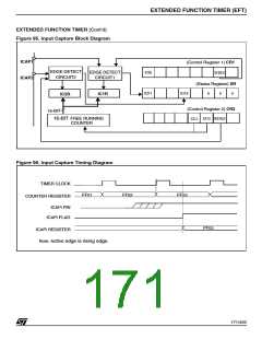
– A timer interrupt is generated if:
– TOIE bit of the CR1 register is set
– EFTIS bit of the CR3 register is set.
If one of these conditions is false, the interrupt re-
mains pending to be issued as soon as they are
both true.
168/426
9

 STMICROELECTRONICS [ ST ]