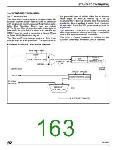
STANDARD TIMER (STIM)
STANDARD TIMER (Cont’d)
10.2.2 Functional Description
10.2.2.1 Timer/Counter control
10.2.2.3 Standard Timer Output Modes
Start-stop Count. The ST-SP bit (STC.7) is used
in order to start and stop counting. An instruction
which sets this bit will cause the Standard Timer to
start counting at the beginning of the next instruc-
tion. Resetting this bit will stop the counter.
OUTPUT modes are selected using 2 bits of the
STC register: OUTMD1 and OUTMD2.
No Output Mode (OUTMD1 = “0”, OUTMD2 = “0”)
The output is disabled and the corresponding pin
is set high, in order to allow other alternate func-
tions to use the I/O pin.
If the counter is stopped and restarted, counting
will resume from the value held at the stop condi-
tion, unless a new constant has been entered in
the Standard Timer registers during the stop peri-
od. In this case, the new constant will be loaded as
soon as counting is restarted.
Square Wave Output Mode (OUTMD1 = “0”,
OUTMD2 = “1”)
The Standard Timer toggles the state of the
STOUT pin on every End Of Count condition. With
INTCLK = 24MHz, this allows generation of a
square wave with a period ranging from 333ns
(STP = STH = STL = 00h) to 5.59 seconds (STP =
STH = STL = FFh).
A new constant can be written in STH, STL, STP
registers while the counter is running. The new
value of the STH and STL registers will be loaded
at the next End of Count condition, while the new
value of the STP register will be loaded immedi-
ately.
PWM Output Mode (OUTMD1 = “1”)
The value of the OUTMD2 bit is transferred to the
STOUT output pin at the End Of Count. This al-
lows the user to generate PWM signals, by modi-
fying the status of OUTMD2 between End of Count
events, based on software counters decremented
on the Standard Timer interrupt.
WARNING:Inordertopreventincorrectcountingof
theStandardTimer,theprescaler(STP)andcounter
(STL, STH) registers must be initialised before the
starting of the timer. If this is not done, counting will
start with the reset values (STH=FFh, STL=FFh,
STP=FFh).
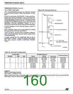
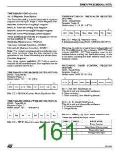
10.2.3 Interrupt Selection
Single/Continuous Mode.
The S-C bit (STC.6) selects between the Single or
Continuous mode.
The Standard Timer may generate an interrupt re-
quest at every End of Count.
Bit 2 of the STC register (INTS) selects the inter-
rupt source between the Standard Timer interrupt
and the external interrupt pin. Thus the Standard
Timer Interrupt uses the interrupt channel and
takes the priority and vector of the external inter-
rupt channel.
SINGLE MODE: at the End of Count, the Standard
Timer stops, reloads the constant and resets the
Start/Stop bit (the user programmer can inspect
the timer current status by reading this bit). Setting
the Start/Stop bit will restart the counter.
CONTINUOUS MODE: At the End of the Count, the
counter automatically reloads the constant and re-
starts.ItisonlystoppedbyresettingtheStart/Stopbit.
If INTS is set to “1”, the Standard Timer interrupt is
disabled; otherwise, an interrupt request is gener-
ated at every End of Count.
The S-C bit can be written either with the timer
stopped or running. It is possible to toggle the S-C
bit and start the Standard Timer with the same in-
struction.
Note: When enabling or disabling the Standard
Timer Interrupt (writing INTS in the STC register)
an edge may be generated on the interrupt chan-
nel, causing an unwanted interrupt.
10.2.2.2 Time Base Generator
To avoid this spurious interrupt request, the INTS
bit should be accessed only when the interrupt log-
ic is disabled (i.e. after the DI instruction). It is also
necessary to clear any possible interrupt pending
requests on the corresponding external interrupt
channel before enabling it. A delay instruction (i.e.
a NOP instruction) must be inserted between the
reset of the interrupt pending bit and the INTS
write instruction.
The INEN bit in the STC register selects the clock
source (refer to RCCU section).
When the INEN bit is reset, INTCLK/4 is selected
as clock input.
When the INEN bit is set, CLOCK2/1024 is select-
ed as clock input. In this case, INMD1 and INMD2
bits in the STC register must always be kept at 0 to
select the event counter mode. This mode allows
the Standard Timer to generate a stable time base
independent from PLL programming.
164/426
9

 STMICROELECTRONICS [ ST ]