EXTENDED FUNCTION TIMER (EFT)
10.3 EXTENDED FUNCTION TIMER (EFT)
10.3.1 Introduction
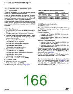
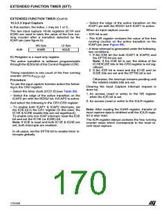
Table 35. EFT Pin Naming conventions
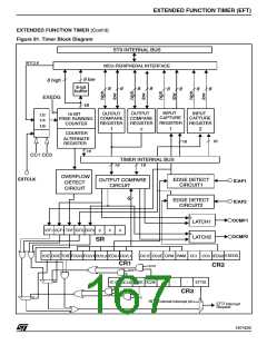
The timer consists of a 16-bit free-running counter
driven by a programmable prescaler.
Function
Input Capture 1 - ICAP1
Input Capture 2 - ICAP2
EFT0
ICAPA0
ICAPB0
EFT1
ICAPA1
ICAPB1
OCMPA1
OCMPB1
It may be used for a variety of purposes, including
pulse length measurement of up to two input sig-
nals (input capture) or generation of up to two out-
put waveforms (output compare and PWM).
Output Compare 1 - OCMP1 OCMPA0
Output Compare 2 - OCMP2 OCMPB0
Pulse lengths and waveform periods can be mod-
ulated from a few microseconds to several milli-
seconds using the timer prescaler and the INTCLK
prescaler.
10.3.3 Functional Description
10.3.3.1 Counter
The principal block of the Programmable Timer is
a 16-bit free running counter and its associated
16-bit registers:
10.3.2 Main Features
■ Programmable prescaler: INTCLK divided by 2,
4 or 8.
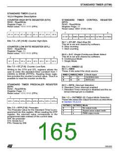
Counter Registers
■ Overflow status flag and maskable interrupts
– Counter High Register (CHR) is the most sig-
nificant byte (MSB).
■ External clock input (must be at least 4 times
slower than the INTCLK clock speed) with the
choice of active edge
– Counter Low Register (CLR) is the least sig-
nificant byte (LSB).
■ Output compare functions with
– 2 dedicated 16-bit registers
Alternate Counter Registers
– Alternate Counter High Register (ACHR) is the
most significant byte (MSB).
– Alternate Counter Low Register (ACLR) is the
least significant byte (LSB).
– 2 dedicated programmable signals
– 2 dedicated status flags
– Maskable interrupt generation
■ Input capture functions with
– 2 dedicated 16-bit registers
These two read-only 16-bit registers contain the
same value but with the difference that reading the
ACLR register does not clear the TOF bit (overflow
flag), (see note page 168).
– 2 dedicated active edge selection signals
– 2 dedicated status flags
Writing in the CLR register or ACLR register resets
the free running counter to the FFFCh value.
– Maskable interrupt generation
■ Pulse width modulation mode (PWM)
■ One pulse mode
■ 5 alternate functions on I/O ports
■ Global Timer interrupt (EFTI).
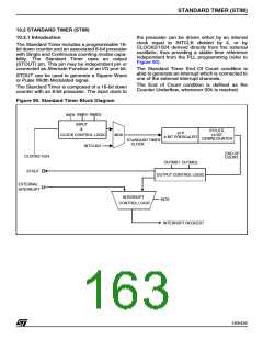
The Block Diagram is shown in Figure 91.
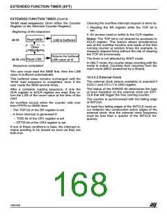
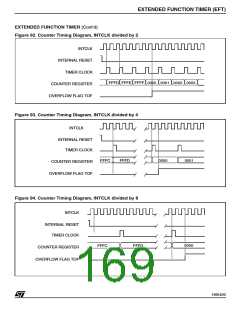
The timer clock depends on the clock control bits
of the CR2 register, as illustrated in Table 36. The
value in the counter register repeats every
131.072, 262.144 or 524.288 INTCLK cycles de-
pending on the CC[1:0] bits.
166/426
9

 STMICROELECTRONICS [ ST ]