EXTENDED FUNCTION TIMER (EFT)
EXTENDED FUNCTION TIMER (Cont’d)
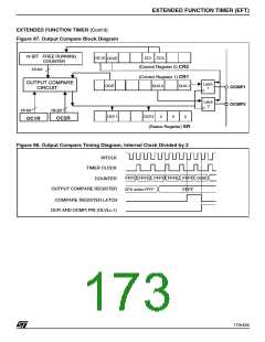
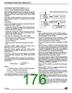
10.3.3.4 Output Compare
– A timer interrupt is generated under the following
two conditions :
1. If the OCIE bit (for both OCMP1 & OCMP2)
and the EFTIS bit are set.
In this section, the index, i, may be 1 or 2.
This function can be used to control an output
waveform or indicating when a period of time has
elapsed.
Note: If the OCIE bit is set, the status of the
OC1IE/OC2IE bits in the CR3 register is not
significant.
When a match is found between the Output Com-
pare register and the free running counter, the out-
put compare function:
2. If the OCIE bit is reset and the OC1IE and /or
OC2IE bits are set and the EFTIS bit is set.
– Assigns pins with a programmable value if the
Otherwise, the interrupt remains pending until
the related enable bits are set.
OCiE bit is set
– Sets a flag in the status register
– Generates an interrupt if enabled
Clearing the output compare interrupt request is
done by:
Two 16-bit registers Output Compare Register 1
(OC1R) and Output Compare Register 2 (OC2R)
contain the value to be compared to the free run-
ning counter each timer clock cycle.
– An access (read or write) to the SR register while
the OCFi bit is set.
– An access (read or write) to the OCiLR register.
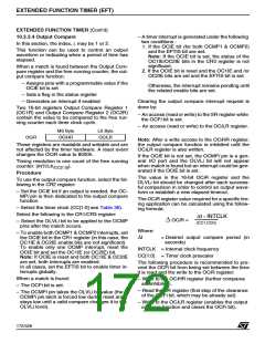
MS Byte
LS Byte
OCiR
OCiHR
OCiLR
Note: After a write access to the OCiHR register,
the output compare function is inhibited until the
OCiLR register is also written.
These registers are readable and writable and are
not affected by the timer hardware. A reset event
changes the OCiR value to 8000h.
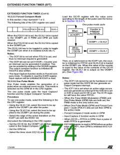
If the OCiE bit is not set, the OCMPi pin is a gen-
eral I/O port and the OLVLi bit will not appear
when match is found but an interrupt could be gen-
erated if the OCIE bit is set.
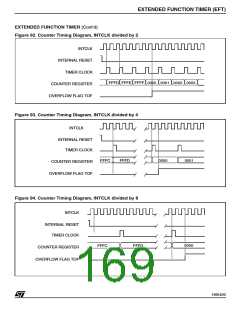
Timing resolution is one count of the free running
counter: (INTCLK
).
CC[1:0]
/
Procedure
The value in the 16-bit OCiR register and the
OLVLi bit should be changed after each success-
ful comparison in order to control an output wave-
form or establish a new elapsed timeout.
To use the output compare function, select the fol-
lowing in the CR2 register:
– Set the OCiE bit if an output is needed, the OC-
MPi pin is then dedicated to the output compare
function.
The OCiR register value required for a specific tim-
ing application can be calculated using the follow-
ing formula:
– Select the timer clock (CC[1:0] see Table 36).
Select the following in the CR1/CR3 register:
∆t INTCLK
(CC1.CC0)
*
∆ OCiR =
– Select the OLVLi bit to be applied to the OCMP
pins after the match occurs.
Where:
– To enable both OCMP1 & OCMP2 interrupts, set
the OCIE bit in the CR1 register (in this case, the
OC1IE & OC2IE enable bits are not significant).
To enable only one OCMP interrupt, reset the
OCIE bit and set the OC1IE (or OC2IE) bit.
Note: If OCIE is reset and both OC1IE & OC2IE
are set, both interrupts are enabled.
∆t
= Desired output compare period (in
seconds)
INTCLK = Internal clock frequency
CC[1:0] = Timer clock prescaler
The following procedure is recommended to pre-
vent the OCFi bit from being set between the time
it is read and the write to the OCiR register:
In all cases, set the EFTIS bit to enable timer in-
terrupts globally.
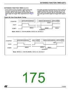
When a match is found:
– Write to the OCiHR register (further compares
are inhibited).
– The OCFi bit is set.
– Read the SR register (first step of the clearance
– The OCMPi pin takes the OLVLi bit value (the
OCMPi pin latch is forced low during reset and
stays low until a valid compare changes it to the
OLVLi level).
of the OCFi bit, which may be already set).
– Write to the OCiLR register (enables the output
compare function and clears the OCFi bit).
172/426
9

 STMICROELECTRONICS [ ST ]