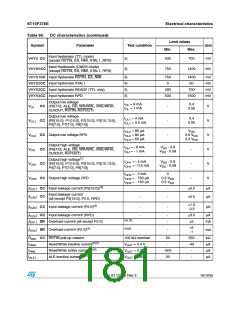
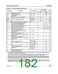
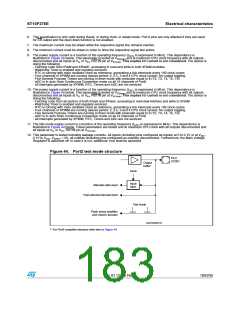
ST10F276E
Electrical characteristics
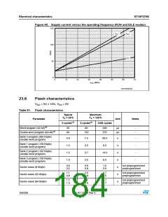
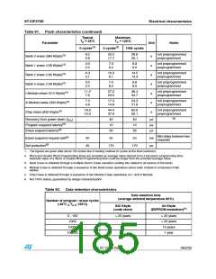
Table 91. Flash characteristics (continued)
Typical
Maximum
TA = 125°C
TA = 25°C
Parameter
Unit
Notes
0 cycles(1)
0 cycles(1)
100k cycles
8.2
5.8
20.2
17.7
28.6
26.1
not preprogrammed
preprogrammed
Bank 0 erase (384 Kbyte)(3)
s
s
s
s
s
s
s
3.0
2.2
7.0
6.2
9.8
9.0
not preprogrammed
preprogrammed
Bank 1 erase (128 Kbyte)(3)
4.3
3.1
10.3
9.1
14.5
13.3
not preprogrammed
preprogrammed
Bank 2 erase (192 Kbyte)(3)
3.0
2.2
7.0
6.2
9.8
9.0
not preprogrammed
preprogrammed
Bank 3 erase (128 Kbyte)(3)
11.2
7.6
27.2
23.5
38.4
34.7
not preprogrammed
preprogrammed
I-Module erase (512 Kbyte)(4)
7.3
4.9
17.3
14.8
24.3
21.8
not preprogrammed
preprogrammed
X-Module erase (320 Kbyte)(4)
18.5
12.0
44.4
37.9
62.6
56.1
not preprogrammed
preprogrammed
Chip erase (832 Kbyte)(5)
(6)
Recovery from power-down (tPD
Program suspend latency(6)
Erase suspend latency(6)
)
-
-
-
40
10
30
40
10
30
μs
μs
μs
Min delay between two
requests
Erase suspend request rate(6)
20
40
20
20
ms
µs
Set protection(6)
170
170
1. The figures are given after about 100 cycles due to testing routines (0 cycles at the final customer).
2. Word and Double Word Programming times are provided as average value derived from a full sector programming time:
Absolute value of a Word or Double Word Programming time could be longer than the provided average value.
3. Bank Erase is obtained through a multiple Sector Erase operation (setting bits related to all sectors of the bank).
4. Module Erase is obtained through a sequence of two Bank Erase operations (since each module is composed of two
banks).
5. Chip Erase is obtained through a sequence of two Module Erase operations on I- and X-Module.
6. Not 100% tested, guaranteed by design characterization
.
Table 92. Data retention characteristics
Data retention time
(average ambient temperature 60°C)
Number of program / erase cycles
(-40°C < TA < 125°C)
832 Kbyte
(code store)
64 Kbyte
(EEPROM emulation)(1)
0 - 100
1000
> 20 years
> 20 years
> 20 years
10 years
1 year
-
-
-
10000
100000
Doc ID 12303 Rev 3
185/235

 STMICROELECTRONICS [ ST ]