Register set
ST10F276E
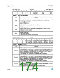
Note:
1
2
BTYP (bit 6 and 7) is set according to the configuration of the bit l6 and l7 of PORT0 latched
at the end of the reset sequence.
BUSCON0 is initialized with 0000h, if EA pin is high during reset. If EA pin is low during
reset, bit BUSACT0 and ALECTRL0 are set (‘1’) and bit field BTYP is loaded with the bus
configuration selected via PORT0.
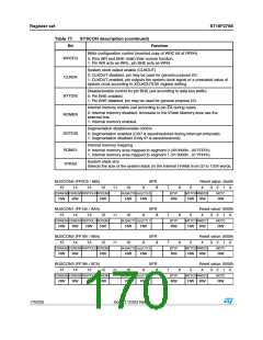
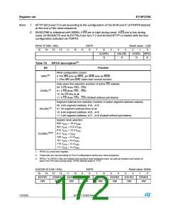
RP0H (F108h / 84h)
15 14 13
ESFR
8
Reset value: --XXh
12
11
10
9
7
6
CLKSEL
R
5
4
3
2
1
0
-
SALSEL
R
CSSEL WRC
R
R
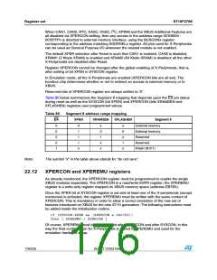
Table 79. RPOH description(1)
Bit
Function
Write configuration control
0: Pin WR acts as WRL, pin BHE acts as WRH
1: Pins WR and BHE retain their normal function
WRC(2)
Chip select line selection (number of active CS outputs)
00: 3 CS lines: CS2...CS0
CSSEL(2)
01: 2 CS lines: CS1...CS0
10: No CS line at all
11: 5 CS lines: CS4...CS0 (Default without pull-downs)
Segment address line selection (number of active segment address outputs)
00: 4-bit segment address: A19...A16
SALSEL(2)
01: No segment address lines at all
10: 8-bit segment address: A23...A16
11: 2-bit segment address: A17...A16 (Default without pull-downs)
System clock selection
000: fCPU = 16 x fOSC
001: fCPU = 0.5 x fOSC
010: fCPU = 10 x fOSC
CLKSEL(2)(3) 011: fCPU = fOSC
100: fCPU = 5 x fOSC
101: fCPU = 8 x fOSC
110: fCPU = 3 x fOSC
111: fCPU = 4 x fOSC
1. RP0H is a read-only register.
2. These bits are set according to Port 0 configuration during any reset sequence.
3. RP0H.7 to RP0H.5 bits are loaded only during a long hardware reset. As pull-up resistors are active on
each Port P0H pins during reset, RP0H default value is “FFh”.
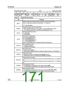
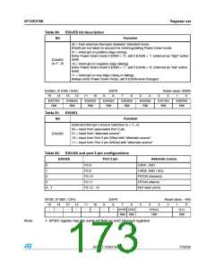
EXICON (F1C0h / E0h)
15 14 13 12
ESFR
8
Reset value: 0000h
11
10
9
7
6
5
4
3
2
1
0
EXI7ES
RW
EXI6ES
RW
EXI5ES
RW
EXI4ES
RW
EXI3ES
RW
EXI2ES
RW
EXI1ES
RW
EXI0ES
RW
172/235
Doc ID 12303 Rev 3

 STMICROELECTRONICS [ ST ]