ST10F276E
Register set
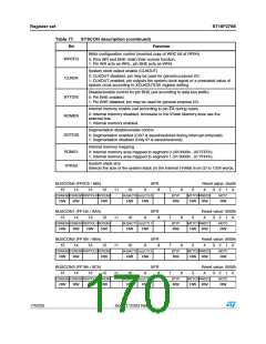
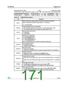
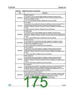
BUSCON4 (FF1Ah / 8Dh)
15 14 13
SFR
Reset value: 0000h
12
11
10
9
8
7
6
5
4
3
2
1
0
CSWEN4CSREN4 RDYPOL4 RDYEN4
-
BUSACT4 ALECTL4
-
BTYP
MTTC4 RWDC4
MCTC
RW
RW
RW
RW
RW
RW
RW RW
RW
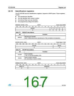
Table 78. BUSCON4 description
Bit
Function
Memory cycle time control (number of memory cycle time wait-states)
0000: 15 wait-states (Number of wait-states = 15 - [MCTC]).
. . .
MCTC
1111: No wait-states.
Read/Write delay control for BUSCONx
RWDCx
MTTCx
0: With read/write delay, the CPU inserts 1 TCL after falling edge of ALE.
1: No read/write delay, RW is activated after falling edge of ALE.
Memory tristate time control
0: 1 wait-state.
1: No wait-state.
External bus configuration
00: 8-bit Demultiplexed Bus
01: 8-bit Multiplexed Bus
10: 16-bit Demultiplexed Bus
11: 16-bit Multiplexed Bus
BTYP
Note: For BUSCON0 BTYP is defined via PORT0 during reset.
ALE lengthening control
ALECTLx
BUSACTx
RDYENx
0: Normal ALE signal.
1: Lengthened ALE signal.
Bus active control
0: External bus disabled.
1: External bus enabled (within the respective address window, see ADDRSEL).
Ready input enable
0: External bus cycle is controlled by bit field MCTC only.
1: External bus cycle is controlled by the READY input signal.
Ready active level control
0: Active level on the READY pin is low, bus cycle terminates with a ‘0’ on READY
pin.
RDYPOLx
1: Active level on the READY pin is high, bus cycle terminates with a ‘1’ on READY
pin.
Read chip select enable
CSRENx
CSWENx
0: The CS signal is independent of the read command (RD).
1: The CS signal is generated for the duration of the read command.
Write chip select enable
0: The CS signal is independent of the write command (WR, WRL, WRH).
1: The CS signal is generated for the duration of the write command.
Doc ID 12303 Rev 3
171/235

 STMICROELECTRONICS [ ST ]