ST10F276E
Register set
22.11
System configuration registers
The ST10F276E has registers used for a different configuration of the overall system. These
registers are described below.
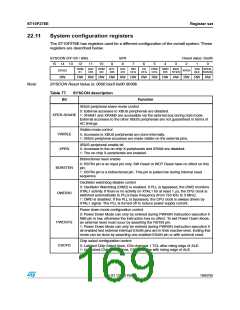
SYSCON (FF12h / 89h)
15 14 13 12
SFR
8
Reset value: 0xx0h
11
10
9
7
6
5
4
3
2
1
0
ROM
S1
SGT
DIS
ROM
EN
BYT
DIS
CLK
EN
WR
CFG
CS
CFG
PWD OWD
CFG DIS
BDR
STEN
VISI XPER-
BLE SHARE
STKSZ
XPEN
RW
RW RW RW RW RW RW RW RW RW RW RW RW RW
Note:
SYSCON Reset Value is: 0000 0xx0 0x00 0000b
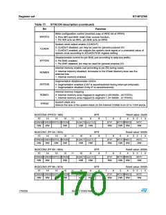
Table 77. SYSCON description
Bit
Function
XBUS peripheral share mode control
0: External accesses to XBUS peripherals are disabled.
1: XRAM1 and XRAM2 are accessible via the external bus during hold mode.
External accesses to the other XBUS peripherals are not guaranteed in terms of
AC timings.
XPER-SHARE
Visible mode control
VISIBLE
XPEN
0: Accesses to XBUS peripherals are done internally.
1: XBUS peripheral accesses are made visible on the external pins.
XBUS peripheral enable bit
0: Accesses to the on-chip X-peripherals and XRAM are disabled.
1: The on-chip X-peripherals are enabled.
Bidirectional reset enable
0: RSTIN pin is an input pin only. SW Reset or WDT Reset have no effect on this
pin.
1: RSTIN pin is a bidirectional pin. This pin is pulled low during internal reset
sequence.
BDRSTEN
OWDDIS
Oscillator watchdog disable control
0: Oscillator Watchdog (OWD) is enabled. If PLL is bypassed, the OWD monitors
XTAL1 activity. If there is no activity on XTAL1 for at least 1 μs, the CPU clock is
switched automatically to PLL’s base frequency (from 750 kHz to 3 MHz).
1: OWD is disabled. If the PLL is bypassed, the CPU clock is always driven by
XTAL1 signal. The PLL is turned off to reduce power supply current.
Power down mode configuration control
0: Power Down Mode can only be entered during PWRDN instruction execution if
NMI pin is low, otherwise the instruction has no effect. To exit Power Down Mode,
an external reset must occur by asserting the RSTIN pin.
1: Power Down Mode can only be entered during PWRDN instruction execution if
all enabled fast external interrupt EXxIN pins are in their inactive level. Exiting this
mode can be done by asserting one enabled EXxIN pin or with external reset.
PWDCFG
CSCFG
Chip select configuration control
0: Latched Chip Select lines, CSx changes 1 TCL after rising edge of ALE.
1: Unlatched Chip Select lines, CSx changes with rising edge of ALE.
Doc ID 12303 Rev 3
169/235

 STMICROELECTRONICS [ ST ]