Functional description
powerSTEP01
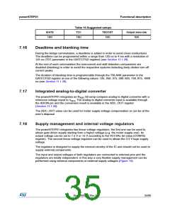
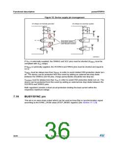
Figure 15. Device supply pin management
All voltages are internally generated
All voltages are externally supplied
VBOOT
VBOOT
CP
CP
VBUS
VBUS
VS
VS
VCC
VSREG
VCC
VSREG
VCC
7V5 - 15V
7V5 - 15V
Using external components
(zener diodes, resistors, ...) it
is possible to reduce internal
power dissipation constrains.
3.3 V
VCCREG
VREG
VCC R E G
VREG
3V3
3V3
AM12834v1
If VCC is externally supplied, the VSREG and VCC pins must be shorted (VSREG must be
compliant with VCC range).
If VREG is externally supplied, the VCCREG and VREG pins must be shorted and equal to
3.3 V.
V
SREG must be always less than VBOOT in order to avoid related ESD protection diode turn-
on. The device can be protected from this event by adding an external low drop diode
between the VSREG and VS pins, charge pump diodes should be low drop too.
V
CCREG must be always less than VCC in order to avoid ESD protection diode turn-on. The
device can be protected from this event by adding an external low drop diode between the
VCCREG and VSREG pins.
Both regulators provide a short circuit protection limiting the load current within the
respective maximum ratings.
7.19
BUSY/SYNC pin
This pin is an open-drain output which can be used as busy flag or synchronization signal
according to the SYNC_EN bit value (STEP_MODE register) (see Section 11.1.23).
36/90
DocID025022 Rev 1

 STMICROELECTRONICS [ ST ]