powerSTEP01
Functional description
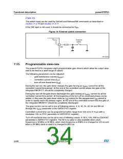
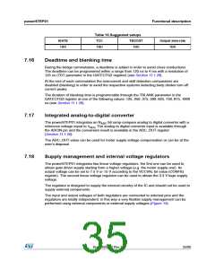
Table 10.Suggested setups
IGATE
TCC
TBOOST
Output slew-rate
TBD
TBD
TBD
TBD
7.16
Deadtime and blanking time
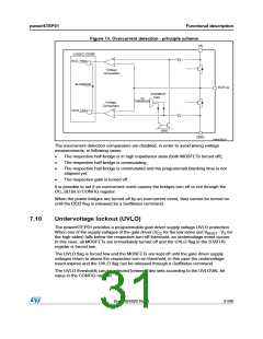
During the bridge commutation, a deadtime is added in order to avoid cross conductions.
The deadtime can be programmed within a range from 125 ns to 4 ms with a resolution of
125 ns (TDT parameter in the GATECFG2 register) (see Section 11.1.26).
At the end of each commutation the overcurrent and stall detection comparators are
disabled (blanking) in order to avoid the respective systems detecting body diodes turn-off
current peaks.
The duration of blanking time is programmable through the TBLANK parameter in the
GATECFG2 register at one of the following values: 125, 250, 375, 500, 625, 750, 875, 1000
ns (see Section 11.1.26).
7.17
7.18
Integrated analog-to-digital converter
The powerSTEP01 integrates an NADC bit ramp-compare analog to digital converter with a
reference voltage equal to VREG. The analog to digital converter input is available through
the ADCIN pin and the conversion result is available in the ADC_OUT register
(Section 11.1.20).
The ADC_OUT value can be used for motor supply voltage compensation or can be at the
user’s disposal.
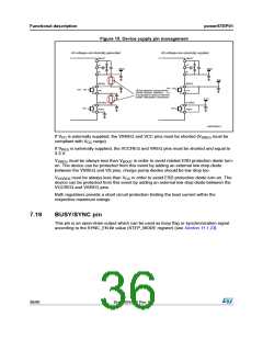
Supply management and internal voltage regulators
The powerSTEP01 integrates two linear voltage regulators: the first one can be used to
obtain gate driver supply starting from a higher voltage (e.g. the motor supply one). Its
output voltage can be set to 7.5 V or 15 V according to the VCCVAL bit value (CONFIG
register). The second linear voltage regulator can be used to obtain the 3.3 V logic supply
voltage.
The regolator is designed to supply the internal circuitry of the IC and should not be used to
supply external components.
The input and output voltages of both regulators are connected to external pins and the
regulators are totally independent: in this way a very flexible supply management can be
performed using external components or external supply voltages (Figure 15).
DocID025022 Rev 1
35/90

 STMICROELECTRONICS [ ST ]