Functional description
powerSTEP01
(Table 41).
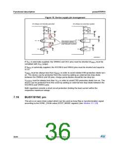
The switch input can be used by GoUntil and ReleaseSW commands as described in
Section 11.2.10 and Section 11.2.11.
If the SW input is not used, it should be connected to VDD
.
Figure 14. External switch connection
VDD
External
switch
SW
AM12833v1
7.15
Programmable slew-rate
The powerSTEP01 integrates eight programmable gate drivers which allow the output slew-
rate to be fixed in a wide range of values.
The following parameters can be adjusted:
–
–
–
gate sink/source current (IGATE
controlled current time (tCC
turn-off over-boost time (tOB).
)
)
During the turn-on, the gate driver charges the gate forcing an IGATE current for all the
controlled current time period. At the end of the controlled current phase the gate of the
integrated MOSFET should be completely charged.
During the turn-off the gate driver discharges the gate sinking an IGATE current for all the
controlled current time period. At the beginning of the turn-off an overboost phase can be
added: in this case the gate driver sinks an IOB current for the programmed tOB period in
order to rapidly reach the plateau region. At the end of the controlled current time the gate of
the integrated MOSFET should be completely discharged.
The gate current can be set to one of following values: 4, 8, 16, 24, 32, 64 and 96 mA
through the IGATE parameter in the GATECFG1 register.
Controlled current time can be programmed within range from 125 ns to 3.75 μs with a
resolution 125 ns (TCC parameter in GATECFG1 register).
Turn-off overboost time can be set to one of following values: 0, 62.5, 125, 250 ns (TBOOST
parameter in GATECFG1 register). The 62.5 ns value is only available when clock
frequency is 16 MHz or 32 MHz; when clock frequency is 8 MHz it is changed to 125 ns and
when a 24 MHz clock is used it is changed to 83.3 ns.
34/90
DocID025022 Rev 1

 STMICROELECTRONICS [ ST ]