NAND128-A, NAND256-A, NAND512-A, NAND01G-A
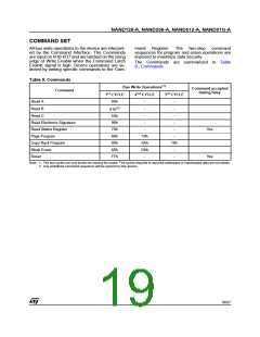
COMMAND SET
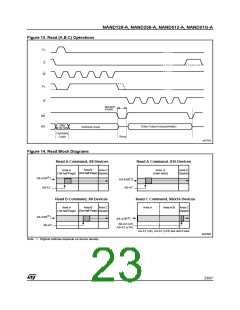
All bus write operations to the device are interpret-
ed by the Command Interface. The Commands
are input on I/O0-I/O7 and are latched on the rising
edge of Write Enable when the Command Latch
Enable signal is high. Device operations are se-
lected by writing specific commands to the Com-
mand Register. The two-step command
sequences for program and erase operations are
imposed to maximize data security.
The Commands are summarized in Table
9., Commands.
Table 9. Commands
(1)
Bus Write Operations
Command accepted
during busy
Command
st
nd
rd
1
CYCLE
2
CYCLE
3
CYCLE
Read A
Read B
00h
-
-
-
-
(2)
01h
Read C
50h
90h
70h
80h
00h
60h
FFh
-
-
-
Read Electronic Signature
Read Status Register
Page Program
Copy Back Program
Block Erase
-
-
-
Yes
Yes
10h
8Ah
D0h
-
-
10h
-
-
Reset
Note: 1. The bus cycles are only shown for issuing the codes. The cycles required to input the addresses or input/output data are not shown.
2. Any undefined command sequence will be ignored by the device.
19/57

 STMICROELECTRONICS [ ST ]