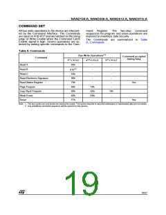
NAND128-A, NAND256-A, NAND512-A, NAND01G-A
MEMORY ARRAY ORGANIZATION
The memory array is made up of NAND structures
where 16 cells are connected in series.
The Bad Block Information is written prior to ship-
ping (refer to Bad Block Management section for
more details).
Table 4. shows the minimum number of valid
blocks in each device. The values shown include
both the Bad Blocks that are present when the de-
vice is shipped and the Bad Blocks that could de-
velop later on.
These blocks need to be managed using Bad
Blocks Management, Block Replacement or Error
Correction Codes (refer to SOFTWARE ALGO-
RITHMS section).
The memory array is organized in blocks where
each block contains 32 pages. The array is split
into two areas, the main area and the spare area.
The main area of the array is used to store data
whereas the spare area is typically used to store
Error correction Codes, software flags or Bad
Block identification.
In x8 devices the pages are split into a main area
with two half pages of 256 Bytes each and a spare
area of 16 Bytes. In the x16 devices the pages are
split into a 256 Word main area and an 8 Word
spare area. Refer to Figure 10., Memory Array Or-
ganization.
Table 4. Valid Blocks
Density of Device
1Gbit
Min
Max
8192
4096
2048
1024
Bad Blocks
8032
4016
2008
1004
The NAND Flash 528 Byte/ 264 Word Page devic-
es may contain Bad Blocks, that is blocks that con-
tain one or more invalid bits whose reliability is not
guaranteed. Additional Bad Blocks may develop
during the lifetime of the device.
512Mbits
256Mbits
128Mbits
Figure 10. Memory Array Organization
x8 DEVICES
x16 DEVICES
Block = 32 Pages
Block = 32 Pages
Page = 528 Bytes (512+16)
Page = 264 Words (256+8)
1st half Page 2nd half Page
Main Area
(256 bytes)
(256 bytes)
Block
Page
Block
Page
8 bits
16 bits
256 Words
512 Bytes
16
Bytes
8
Words
Page Buffer, 264 Words
8
Page Buffer, 512 Bytes
16
256 Words
Words
512 Bytes
16 bits
Bytes
8 bits
AI07587
15/57

 STMICROELECTRONICS [ ST ]