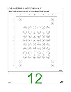
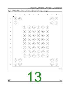
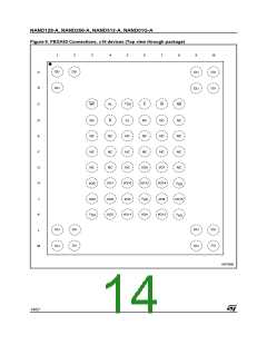
NAND128-A, NAND256-A, NAND512-A, NAND01G-A
SIGNAL DESCRIPTIONS
See Figure 2., Logic Diagram, and Table
3., Signal Names, for a brief overview of the sig-
nals connected to this device.
tions. Data is valid tRLQV after the falling edge of R.
The falling edge of R also increments the internal
column address counter by one.
Inputs/Outputs (I/O0-I/O7). Input/Outputs 0 to 7
are used to input the selected address, output the
data during a Read operation or input a command
or data during a Write operation. The inputs are
latched on the rising edge of Write Enable. I/O0-I/
O7 are left floating when the device is deselected
or the outputs are disabled.
Write Enable (W). The Write Enable input, W,
controls writing to the Command Interface, Input
Address and Data latches. Both addresses and
data are latched on the rising edge of Write En-
able.
During power-up and power-down a recovery time
of 1µs (min) is required before the Command Inter-
face is ready to accept a command. It is recom-
mended to keep Write Enable high during the
recovery time.
Inputs/Outputs (I/O8-I/O15). Input/Outputs 8 to
15 are only available in x16 devices. They are
used to output the data during a Read operation or
input data during a Write operation. Command and
Address Inputs only require I/O0 to I/O7.
The inputs are latched on the rising edge of Write
Enable. I/O8-I/O15 are left floating when the de-
vice is deselected or the outputs are disabled.
Write Protect (WP). The Write Protect pin is an
input that gives a hardware protection against un-
wanted program or erase operations. When Write
Protect is Low, VIL, the device does not accept any
program or erase operations.
It is recommended to keep the Write Protect pin
Low, VIL, during power-up and power-down.
Address Latch Enable (AL). The Address Latch
Enable activates the latching of the Address inputs
in the Command Interface. When AL is high, the
inputs are latched on the rising edge of Write En-
able.
Ready/Busy (RB). The Ready/Busy output, RB,
is an open-drain output that can be used to identify
if the P/E/R Controller is currently active.
When Ready/Busy is Low, VOL, a read, program or
erase operation is in progress. When the operation
Command Latch Enable (CL). The Command
Latch Enable activates the latching of the Com-
mand inputs in the Command Interface. When CL
is high, the inputs are latched on the rising edge of
Write Enable.
completes Ready/Busy goes High, VOH
.
The use of an open-drain output allows the Ready/
Busy pins from several memories to be connected
to a single pull-up resistor. A Low will then indicate
that one, or more, of the memories is busy.
Refer to the Ready/Busy Signal Electrical Charac-
teristics section for details on how to calculate the
value of the pull-up resistor.
Chip Enable (E). The Chip Enable input acti-
vates the memory control logic, input buffers, de-
coders and sense amplifiers. When Chip Enable is
low, VIL, the device is selected.
While the device is busy programming or erasing,
Chip Enable transitions to High, VIH, are ignored
and the device does not revert to the Standby
mode.
V
DD Supply Voltage. VDD provides the power
supply to the internal core of the memory device.
It is the main power supply for all operations (read,
program and erase).
While the device is busy reading:
An internal voltage detector disables all functions
whenever VDD is below 2.5V (for 3V devices) or
1.5V (for 1.8V devices) to protect the device from
any involuntary program/erase during power-tran-
sitions.
Each device in a system should have VDD decou-
pled with a 0.1µF capacitor. The PCB track widths
should be sufficient to carry the required program
and erase currents
■
the Chip Enable input should be held Low
during the whole busy time (tBLBH1) for
devices that do not present the Chip Enable
Don’t Care option. Otherwise, the read
operation in progress is interrupted and the
device reverts to the Standby mode.
for devices that feature the Chip Enable Don't
Care option, Chip Enable going High during
the busy time (tBLBH1) will not interrupt the
read operation and the device will not revert to
the Standby mode.
■
V
SS Ground. Ground, VSS, is the reference for
the power supply. It must be connected to the sys-
tem ground.
Read Enable (R). The Read Enable, R, controls
the sequential data output during Read opera-
16/57

 STMICROELECTRONICS [ ST ]