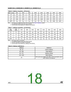
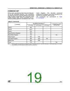
NAND128-A, NAND256-A, NAND512-A, NAND01G-A
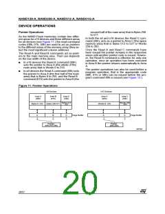
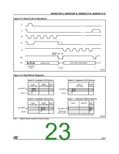
Read Memory Array
Once a read command is issued three types of op-
erations are available: Random Read, Page Read
and Sequential Row Read.
Each operation to read the memory area starts
with a pointer operation as shown in the Pointer
Operations section. Once the area (main or spare)
has been selected using the Read A, Read B or
Read C commands four bus cycles (for 512Mb
and 1Gb devices) or three bus cycles (for 128Mb
and 256Mb devices) are required to input the ad-
dress (refer to Table 6.) of the data to be read.
Random Read. Each time the command is is-
sued the first read is Random Read.
Page Read. After the Random Read access the
page data is transferred to the Page Buffer in a
time of t
(refer to Table 21. for value). Once
WHBH
The device defaults to Read A mode after power-
up or a Reset operation.
When reading the spare area addresses:
the transfer is complete the Ready/Busy signal
goes High. The data can then be read out sequen-
tially (from selected column address to last column
address) by pulsing the Read Enable signal.
■
A0 to A3 (x8 devices)
A0 to A2 (x16 devices)
■
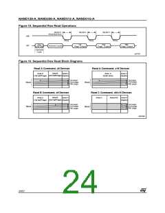
Sequential Row Read. After the data in last col-
umn of the page is output, if the Read Enable sig-
nal is pulsed and Chip Enable remains Low then
the next page is automatically loaded into the
Page Buffer and the read operation continues. A
Sequential Row Read operation can only be used
to read within a block. If the block changes a new
read command must be issued.
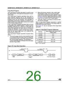
Refer to Figure 15. and Figure 16. for details of Se-
quential Row Read operations.
To terminate a Sequential Row Read operation set
are used to set the start address of the spare area
while addresses:
■
A4 to A7 (x8 devices)
A3 to A7 (x16 devices)
■
are ignored.
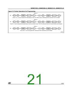
Once the Read A or Read C commands have
been issued they do not need to be reissued for
subsequent read operations as the pointer re-
mains in the respective area. However, the Read
B command is effective for only one operation,
once an operation has been executed in Area B
the pointer returns automatically to Area A and so
another Read B command is required to start an-
other read operation in Area B.
the Chip Enable signal to High for more than tEHEL
.
Sequential Row Read is not available when the
Chip Enable Don't Care option is enabled.
22/57

 STMICROELECTRONICS [ ST ]