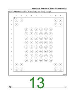
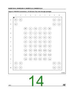
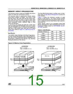
NAND128-A, NAND256-A, NAND512-A, NAND01G-A
BUS OPERATIONS
There are six standard bus operations that control
the memory. Each of these is described in this
section, see Table 5., Bus Operations, for a sum-
mary.
Data is accepted only when Chip Enable is Low,
Address Latch Enable is Low, Command Latch
Enable is Low and Read Enable is High. The data
is latched on the rising edge of the Write Enable
signal. The data is input sequentially using the
Write Enable signal.
Command Input
See Figure 25. and Table 20. and Table 21. for de-
tails of the timings requirements.
Command Input bus operations are used to give
commands to the memory. Command are accept-
ed when Chip Enable is Low, Command Latch En-
able is High, Address Latch Enable is Low and
Read Enable is High. They are latched on the ris-
ing edge of the Write Enable signal.
Data Output
Data Output bus operations are used to read: the
data in the memory array, the Status Register, the
Electronic Signature and the Serial Number.
Only I/O0 to I/O7 are used to input commands.
See Figure 23. and Table 20. for details of the tim-
ings requirements.
Data is output when Chip Enable is Low, Write En-
able is High, Address Latch Enable is Low, and
Command Latch Enable is Low.
Address Input
The data is output sequentially using the Read En-
able signal.
See Figure 26. and Table 21. for details of the tim-
ings requirements.
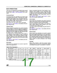
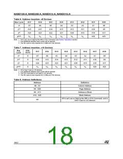
Address Input bus operations are used to input the
memory address. Three bus cycles are required to
input the addresses for the 128Mb and 256Mb de-
vices and four bus cycles are required to input the
addresses for the 512Mb and 1Gb devices (refer
to Tables 6 and 7, Address Insertion).
The addresses are accepted when Chip Enable is
Low, Address Latch Enable is High, Command
Latch Enable is Low and Read Enable is High.
They are latched on the rising edge of the Write
Enable signal. Only I/O0 to I/O7 are used to input
addresses.
Write Protect
Write Protect bus operations are used to protect
the memory against program or erase operations.
When the Write Protect signal is Low the device
will not accept program or erase operations and so
the contents of the memory array cannot be al-
tered. The Write Protect signal is not latched by
Write Enable to ensure protection even during
power-up.
See Figure 24. and Table 20. for details of the tim-
ings requirements.
Standby
Data Input
When Chip Enable is High the memory enters
Standby mode, the device is deselected, outputs
are disabled and power consumption is reduced.
Data Input bus operations are used to input the
data to be programmed.
Table 5. Bus Operations
(1)
Bus Operation
E
AL
CL
R
W
WP
I/O0 - I/O7
I/O8 - I/O15
(2)
V
V
V
V
Command Input
Address Input
Data Input
Rising
Rising
Rising
Command
Address
Data Input
Data Output
X
X
IL
IL
IL
IL
IL
IH
IH
IH
IH
X
V
V
V
V
V
V
V
X
X
X
X
IH
IL
V
IL
V
Data Input
IL
V
IL
V
V
IH
Data Output
Write Protect
Falling
Data Output
IL
V
IL
X
X
X
X
X
X
X
X
X
X
X
V
IH
Standby
X
X
Note: 1. Only for x16 devices.
2. WP must be VIH when issuing a program or erase command.
17/57

 STMICROELECTRONICS [ ST ]