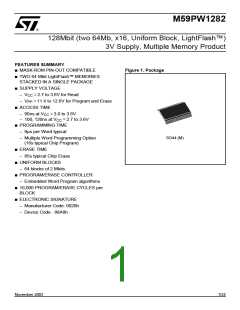
M59PW1282
SUMMARY DESCRIPTION
The M59PW1282 is a 128Mbit (8Mb x16), Mask-
ROM pinout compatible, non-volatile LightFlash™
memory, that can be read, erased and repro-
grammed. Read operations can be performed us-
ing a single low voltage (2.7 to 3.6V) supply.
Program and Erase operations require an addi-
preserve valid data while old data is erased. Pro-
gram and Erase commands are written to the
Command Interface of the memory. An on-chip
Program/Erase Controller (P/E.C.) simplifies the
process of programming or erasing the memory by
taking care of all of the special operations that are
required to update the memory contents.
tional V (11.4 to 12.6V) power supply. On pow-
PP
er-up the memory defaults to its Read mode where
it can be read in the same way as a ROM or
EPROM.
The Mask-ROM compatibility is obtained using a
dual function Address/Voltage Supply pin (A22/
The M59PW1282 features an innovative com-
mand, Multiple Word Program, that is used to pro-
gram large streams of data. It greatly reduces the
total programming time when a large number of
Words are written to the memory at any one time.
Using this command the entire memory can be
programmed in 16s, compared to 72s using the
standard Word Program.
The end of a Program or Erase operation can be
detected and any error conditions identified. The
command set required to control the memory is
consistent with JEDEC standards. Chip Enable
and Output Enable signals control the bus opera-
tion of the memory. They allow simple connection
to most microprocessors, often without additional
logic.
V
). In Read mode the A22/V pin works as an
PP
PP
address pin; in Program or Erase mode it also
works as a voltage supply pin. At the beginning of
any program or erase operation, a specific proce-
dure (see Figure 4) must be performed to internal-
ly memorize the A22 value that will be used during
the program or erase operation.
The device is composed of two 64Mbit memories
stacked in a single package. Recommended oper-
ating conditions do not allow both memories to be
active at the same time. Address A22 selects the
memory to be enabled. The other memory is in
Standby mode.
The memory is offered in SO44 package and is
supplied with all the bits set to ’1’).
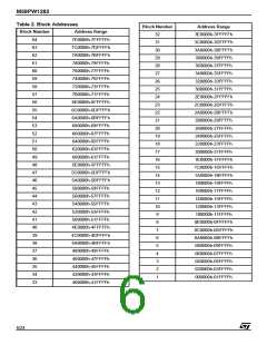
The memory is divided into 64 uniform blocks that
can be erased independently so it is possible to
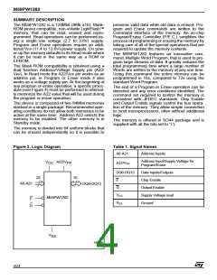
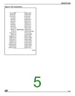
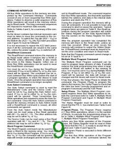
Figure 2. Logic Diagram
Table 1. Signal Names
A0-A21
Address Inputs
Address Input/Supply Voltage for
Program/Erase
V
A22/V
PP
CC
A22/V
PP
DQ0-DQ15
Data Inputs/Outputs
Chip Enable
22
16
E
A0-A21
DQ0-DQ15
G
Output Enable
Supply Voltage read
Ground
V
CC
M59PW1282
E
V
SS
G
V
SS
AI07209
4/24

 STMICROELECTRONICS [ ST ]