L7250
Ω
Ω
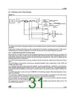
Considering a typical application with Rs = 0.25 , Lm = 0.75mH, Rm = 7.5 , Gs = 4.5 Gpow = 8, Rf = 5.6K, Cc =
3.3nF, Rc = 33k we will obtain a bandwidth about 20kHz. To increase the bandwidth a different values of the external
components could be calculated following the above relation and taking in account the limitation introduced by the
ω
second pole due to the error amplifier bandwidth ( t). This one has a typical value about 4MHz.
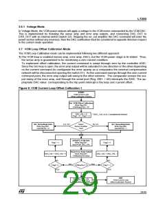
3.1 VCM Operating Modes and Control
At power-on-reset the VCM register is cleared and the VCM is in Unload/Retract mode.
Via serial port is possible to command the following modes: Unload/Retract, Tri-state (disable), Brake, Enable
Current Mode, Enable Voltage Mode, Offset Calibration
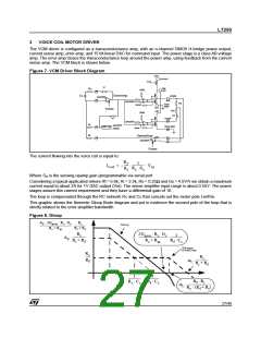
3.2 VCM Power Driver H-Bridge
The VCM driver is capable of high performance linear, class-AB, H-bridge operation with all power devices in-
ternal. The power amp stage is configured as a voltage amp with gain of 16. The H-bridge consists of 4 N-chan-
nel DMOS power transistors. Power is supplied to the H-bridge through the internal ISO-FET ( at pins VM
52,53), and ground returned via four VCMGND pins (5,6,43,44). Boosted gate drive for the high side drivers is
provided by the charge pump circuitry, with the boosted voltage at the VCP pin.
3.3 VCM Current Command 15 bit DAC
The VCM current command is defined by an internal linear, 2's complement, 15 bit DAC. The mid scale refer-
ence for the DAC, VREF25, is defined by an on-chip reference at 2.5V. VREF25 is the reference for the sense
amp and error amp in the VCM loop. Level shifting from VREF25 to VM/2 will be done in the power stage.
0x3FFF Max current flowing from VCMN to VCMP (current mode operation)
0x----
0x0001
0x0000 zero current
0xFFFF
0x----
0x4000 Max current flowing from VCMP to VCMN (current mode operation)
To write the 15 bit DAC the two register REG09H [14:8] and REG0AH [7:0] have to be referred.
At any time the MSB register is entered, to apply the modification also the LSB register must be write. Instead
writing only the LSB register its content will be immediatly visible on the DAC structure.
Then a double write sequence its necessary if the [14:8] bit have to be modified while it is possible to move the
DAC in a fine way (write of the [7:0] bit) with only one write sequence.
3.4 VCM Current Sense Amp
VCM current is sensed by a diff amp that amplifies and level shifts the voltage drop across an external resistor
in series with the VCM coil. The sense amp has a nominal differential voltage gain programmable through the
serial port bit Reg09H bit 7, and the output, VSENSE, is relative to VREF25 (pin 21). The amp has been design
to have high common mode rejection (over 70dB at DC), Power supply rejection over 60dB, and as low an input
offset as possible.
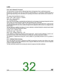
3.5 VCM Current Loop Error Amplifier
The VCM error amp gains up the difference between the current command voltage DAC_OUT and the current
sense voltage VSENSE. VCM current loop compensation is implemented externally with an RC network con-
nected across ERR_IN and ERR_OUT. The error amp output is referred to VREF25.
3.6 Error Amp Output Clamp
The error amp output swing is clamped in both directions (Vref25+/-3Vbe) to prevent wind-up of the integrating
compensation components around the error amp in the event of saturation.
28/46

 STMICROELECTRONICS [ ST ]