L7250
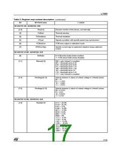
Table 2. Register map content description (continued)
Bit
SPI field name
Content
[5:4]
RLToffBrake[1:0]
Selects the duration of Toff (Ton) active brake phase:
00 = 300usec
01 = 400usec
10 = 500usec
11 = 600usec
[7]
[6]
SkockConf
SkockTh[0]
Selects the Shock Sensor application
0 = piezo element
1 = charging element
Selects the Shock Sensor threshold
0 = Vref +/- 200mV
1 = Vref +/- 500mV
REGISTER CTR1, ADDRESS: 03H
Spstate[3:0]
[3:0]
[6:4]
[7]
0000 = CLCOAST
0001 = OLCOAST
0010 = OLSIX
0011 = OLSIN
0100 = OLBRAKE
0101 = INDSENSE
0110 = CLSIX
0111 = CLSIN
1000 = CLBRAKE
VCMstate[2:0]
Possible states for the VCM:
000 = Unload/Retract
001 = tri-state
010 = brake
011 = enable current mode
100 = enable voltage mode
101 = offset calibration
110 = confirm the previous state
111 = confirm the previous state
BemfOffCal
REGISTER CTR2, ADDRESS: 04H
VCM BEMF processor offset calibration
[1:0]
PWMmask[1:0]
Selects the length of the mask over PWM rising edge:
00 = 2 us
01 = 4 us
10 = 6 us
11 = 8 us
[4:2]
Currdac[2:0]
Selects the voltage threshold for the spindle current limiter:
000 = 250mV
001 = 300mV
010 = 350mV
011 = 400mV
100 = 450mV
101 = 500mV
110 = 550mV
111 = 600mV
18/46

 STMICROELECTRONICS [ ST ]