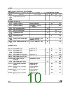
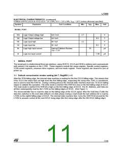
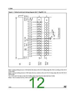
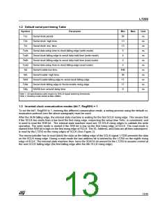
PDF
最近搜索
热门搜索
发布采购

| 型号: | L7250 |
| PDF下载: | 下载PDF文件 查看货源 |
| 内容描述: | 5V和12V的主轴和VCM电机驱动器 [5V & 12V SPINDLE AND VCM MOTORS DRIVER] |
| 分类和应用: | 驱动器电机 |
| 文件页数/大小: | 46 页 / 478 K |
| 品牌: |  STMICROELECTRONICS [ ST ] STMICROELECTRONICS [ ST ] |
专业IC领域供求交易平台:提供全面的IC Datasheet资料和资讯,Datasheet 1000万数据,IC品牌1000多家。