L7250
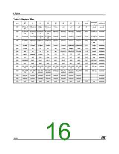
Table 1. Register Map
mnemoni
c
addr
b7
b6
b5
b4
b3
b2
b1
b0
name
attributes
00H
SPNCurrSi VCMcalOut
gn
ZCBad
ThShutdown
ThWarn
rev2
rev1
rev0
SR
status
readonly
01H
02H
03H
RLvoltage1 RLvoltage1 RLvoltage2 RLvoltage2
[1] [0] [1] [0]
Rltimer[2]
Rlcalib[3]
SPstate3
Rltimer[1]
Rlcalib[2]
SPstate2
Rltimer[0]
Rlcalib[1]
SPstate1
NoBrake
Rlcalib[0]
SPstate0
VCM1
VCM2
CTR1
VCM RLreg
VCMRL reg
read/write
read/write
read/write
ShockConf ShockTh[0] RLToffBrake RLToffBrake
[1] [0]
BemfOffCal VCMState2 VCMState1 VCMState0
SP&VCMst
ate
04H
05H
06H
07H
08H
09H
0AH
0BH
SPslew2
SPIprot
w4
SPslew1
m3
SPslew0
m2
Curdac2
m1
Curdac1
m0
Curdac0
TSDen
PWMmask1 PWMmask0
CTR2
CTR3
CTR4
CTR5
KVR
control
control
read/write
read/write
read/write
read/write
read/write
read/write
read/write
readonly
VnegEn
Sken
PREsmo
TO0
w3
w2
w1
w0
PREADC(1) PREADC(0)
control
LoadCP
Kv7
Advance
Kv6
FFWEn
Kv5
TO4
TO3
TO2
Kv2
TO1
Kv1
control
Kv4
Kv3
Kv0
Kval
GainSwitch
dac7
dac14
dac6
dac13
dac5
dac12
dac4
dac11
dac3
dac10
dac2
dac9
dac1
dac8
DAR1
DAR2
ADR
DAC reg 1
DAC reg 2
ADC reg
dac0
ADC_DATA ADC_DATA ADC_DATA ADC_DATA ADC_DATA ADC_DATA ADC_DATA ADC_DATA
(9)
(8)
(7)
(6)
(5)
(4)
(3)
(2)
0CH
ADC_DATA ADC_DATA ADC_RES
ADC_RES ADCRange
_ADDR(0)
ADC_CH_
ADDR(1)
ADC_CH_
ADDR(0)
ADC_START
ADR
ADC reg
read/write
(1)
(0)
_ADDR(1)
reserved
reserved
test5
0DH
0EH
0FH
reserved
reserved
test7
reserved
reserved
test6
reserved
reserved
test4
reserved
reserved
test3
reserved
reserved
test2
reserved
reserved
test1
reserved
reserved
test0
read/write
read/write
read/write
TEST
test
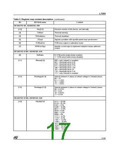
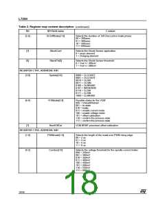
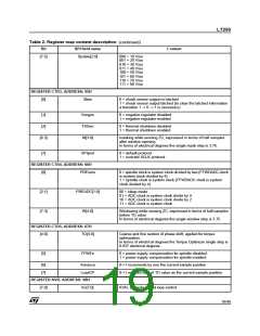
16/46

 STMICROELECTRONICS [ ST ]