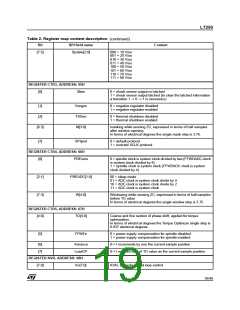
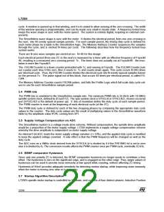
L7250
Table 2. Register map content description (continued)
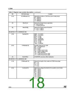
Bit
SPI field name
Content
[7:5]
Spslew[2:0]
000 = 10 V/us
001 = 20 V/us
010 = 30 V/us
011 = 40 V/us
100 = 50 V/us
101 = 60 V/us
110 = 70 V/us
111 = 80 V/us
REGISTER CTR3, ADDRESS: 05H
[0]
Sken
0 = shock sensor output no latched
1 = shock sensor output latched (to clear the latched information
a transition 1 -> 0 -> 1 is necessary)
[1]
[2]
Vnegen
TSDen
M[3:0]
0 = negative regulator disabled
1 = negative regulator enabled
0 = thermal shutdown disabled
1 = thermal shutdown enabled
[6:3]
masking while sensing ZC, expressed in terms of half samples
after window opening
In terms of electrical degrees the single mask step is 3.75.
[7]
SPIprot
0 = default protocol
1 = inverted SCLK protocol
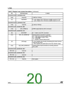
REGISTER CTR4, ADDRESS: 06H
[0]
PREsmo
PREADC[1:0]
W[4:0]
0 = spindle clock is system clock divided by two (FFWDADC clock
is system clock divided by 8)
1 = spindle clock is system clock (FFWDADC clock is system
clock divided by 4)
[2:1]
[7:3]
00 = sleep mode
01 = ADC clock is system clock divide by 4
10 = ADC clock is system clock divide by 2
11 = ADC clock is system clock
Windowing while sensing ZC, expressed in terms of half samples
before TO value
In terms of electrical degrees the single window step is 3.75.
REGISTER CTR5, ADDRESS: 07H
[4:0]
TO[4:0]
Coarse and fine section of phase shift, applied for torque
optimization.
In terms of electrical degrees the Torque Optimizer single step is
0.937 electrical degrees.
[5]
FFWEn
0 = power supply compensation for spindle disabled
1 = power supply compensation for spindle enabled
[6]
[7]
Advance
LoadCP
0->1 increments by one the current sample position
0->1 enables load of TO value as the current sample position
REGISTER KVR, ADDRESS: 08H
[7:0] Kv[7:0]
KVAL factor for speed loop control
19/46

 STMICROELECTRONICS [ ST ]