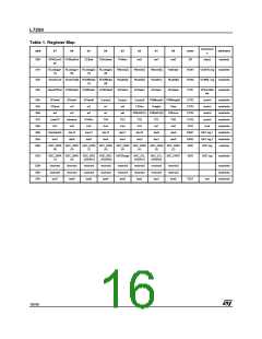
L7250
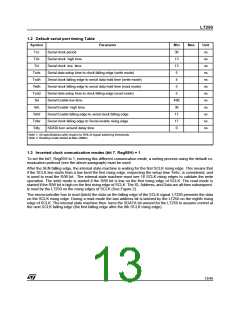
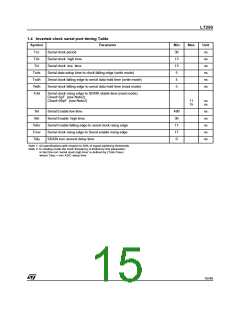
1.2 Default serial port timing Table
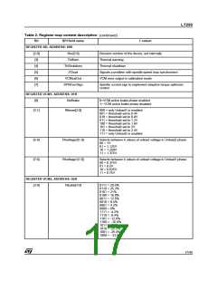
Symbol
Parameter
Min
30
13
13
5
Max
Unit
ns
ns
ns
ns
ns
ns
ns
ns
ns
ns
ns
ns
Tcc
Tch
Serial clock period
Serial clock high time
Serial clock low time
Tcl
Tcds
Tcdh
Tedh
Tcdd
Tel
Serial data setup time to clock falling edge (write mode)
Serial clock falling edge to serial data hold time (write mode)
Serial clock falling edge to serial data hold time (read mode)
Serial data setup time to clock falling edge (read mode)
Serial Enable low time
4
5
5
490
30
17
17
0
Teh
Serial Enable high time
Tefcf
Tcfer
Tdly
Serial Enable falling edge to serial clock falling edge
Serial clock falling edge to Serial enable rising edge
SDATA turn around delay time
Note 1: All specifications with respect to 50% of signal switching thresholds
Note 2: Reading mode tested at Max 20Mhz
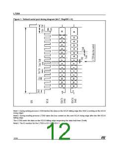
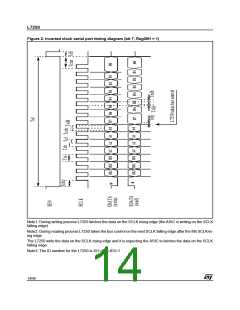
1.3 Inverted clock comunication modes (bit 7, Reg05H) = 1
To set the bit7, Reg05H to 1, entering this different comunication mode, a writing process using the default co-
munication protocol (see the above paragraph) must be used.
After the SEN falling edge, the internal state machine is waiting for the first SCLK rising edge. This means that
if the SCLK line starts from a low level the first rising edge, respecting the setup time Tefcr, is considered, and
is used to read the R/W bit. The internal state machine must see 16 SCLK rising edges to validate the write
operation. The write mode is started if the R/W bit is low on the first rising edge of SCLK. The read mode is
started if the R/W bit is high on the first rising edge of SCLK. The ID, Address, and Data are all then subsequent-
ly read by the L7250 on the rising edges of SCLK (See Figure 2).
The microcontroller has to read (latch) the data on the falling edge of the SCLK signal. L7250 presents the data
on the SCLK rising edge. During a read mode the last address bit is latched by the L7250 on the eighth rising
edge of SCLK. The internal state machine then turns the SDATA bit around for the L7250 to assume control at
the next SCLK falling edge (the first falling edge after the 8th SCLK rising edge).
13/46

 STMICROELECTRONICS [ ST ]