L7250
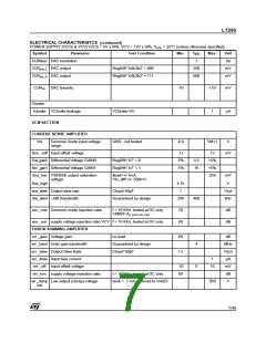
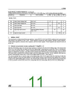
ELECTRICAL CHARACTERISTCS (continued)
POWER SUPPLY [VCC5 & VCV] VCC5 = 5V ±10%, VCV = 12V ±10%. T
= 25°C (unless otherwise specified)
amb
Symbol
Parameter
Test Condition
Min.
Typ.
Max.
Unit
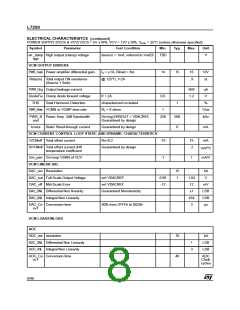
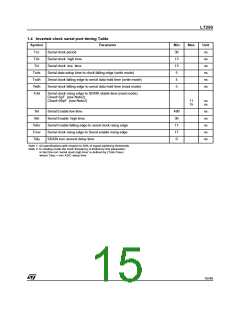
SERIAL PORT
Voh
Vol
Vih
Vil
Logic Output voltage high
Logic Output voltage low
Logic input high
Ioh=1mA
Iol=1mA
Iih=1uA
Iil=-1uA
2.7
2.2
V
V
0.5
0.5
V
Logic input low
V
Iih
Logic high input current
Internal Pulldown Resistor
Vin = 3.3V
33
µA
Iil
Logic low input current
-1.00
µA
1
SERIAL PORT
The serial port is a bidirectional three pin interface, using SDATA, SCLK and SEN to address and communicate
with sixteen 8 bit registers in the L7250. These registers include the status register, Spindle control registers,
VCM control registers, sinewave drive registers, and test mode register. These registers are cleared to zero at
power up.
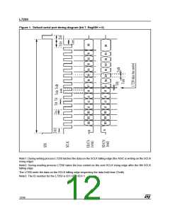
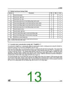
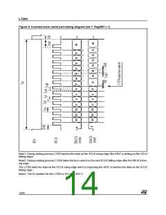
1.1 Default comunication modes setting (bit 7, Reg05H ) = 0
After the SEN falling edge, the internal state machine is waiting for the first SCLK falling edge. This means that
if the SCLK line starts from an high level the first falling edge, respecting the setup time Tefcf, is considered,
and is used to read the R/W bit. During a writing process the internal state machine must see 16 SCLK falling
edges to validate the operation. The write mode is started if the R/W bit is low on the first falling edge of SCLK.
The read mode is started if the R/W bit is high on the first falling edge of SCLK. The ID, Address, and Data are
all then subsequently read by the L7250 on the falling edges of SCLK. (See Figure 1)
The microcontroller has to read the data on the falling edge of the SCLK signal. After the hold time (Tedh) the
data line switches to the next data without a tri-state phase.During a read mode the last address bit is read by
L7250 on the eighth falling edge of SCLK. The internal state machine then turns the SDATA bit around for the
L7250 to assume control at the next SCLK rising edge (the first rising edge after the 8th SCLK falling edge).
11/46

 STMICROELECTRONICS [ ST ]