L7250
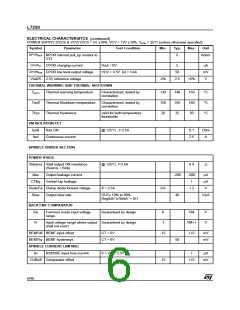
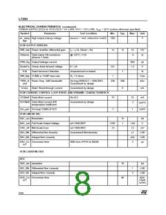
ELECTRICAL CHARACTERISTCS (continued)
POWER SUPPLY [VCC5 & VCV] VCC5 = 5V ±10%, VCV = 12V ±10%. T
= 25°C (unless otherwise specified)
amb
Symbol
Parameter
Test Condition
Isource = 1mA, referred to Vref25
Min.
Typ.
Max.
Unit
err _clamp High output (clamp) voltage
high
TBD
V
VCM OUTPUT DRIVERS
PWR_Gain Power amplifier differential gain.
I = ±1A, Rload = 8Ω
14
15
16
.9
V/V
o
Rds(on) Total output ON resistance
(Source + Sink)
@ 125°C, I=2A
Ω
PWR_Lkg Output leakage current
600
1.2
uA
V
DiodeFw Clamp diode forward voltage
If = 2A
0.6
THD
Total Harmonic Distortion
characterized no tested
1
%
PWR_Slew VCMN or VCMP slew rate
R = 8 ohms
1
V/us
kHz
L
PWR_B Power Amp -3dB Bandwidth
and
Driving ERROUT = VDACREF,
Guaranteed by design
250
500
0
Icross
Static Shoot-through current
Guaranteed by design
mA
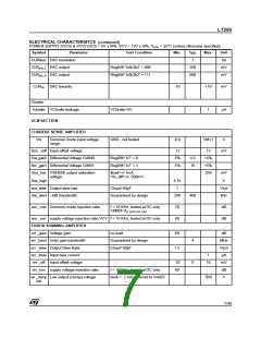
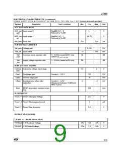
VCM CURRENT CONTROL LOOP STATIC AND DYNAMIC CHARACTERISTICS
IVCMoff Total offset current
Rs=0.2
-75
-1
75
.2
mA
o
DIVCMoff Total offset current drift
temperature coefficient
Guaranteed by design
mA/ C
Gm_psrr Gm loop VSRR of VCV
VCM LINEAR DAC
1
mA/V
DAC_res Resolution
15
1
bit
V
DAC_out Full Scale Output Voltage
DAC_off Mid-Scale Error
wrt VDACREF
0.96
-12
1.04
12
wrt VDACREF
mV
LSB
LSB
µs
DAC_DNL Differential Non linearity
DAC_INL Integral Non Linearity
Guaranteed Monotonicity
±1
±64
3
DAC_Co Conversion time
nvT
90% from 3FFFh to 0020h
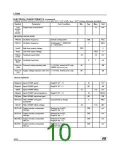
VCM LOAD/UNLOAD
ADC
ADC_res resolution
10
40
bit
ADC_DNL Differential Non Linearity
ADC_INL Integral Non Linearity
1
3
LSB
LSB
ADC_Co Conversion time
nvT
ADC
Clock
cycles
8/46

 STMICROELECTRONICS [ ST ]