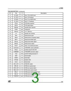
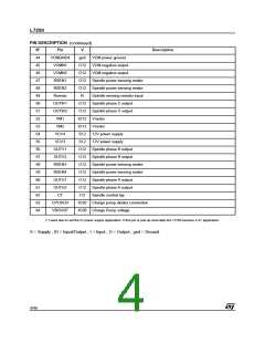
L7250
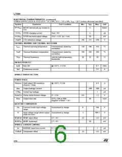
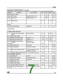
ELECTRICAL CHARACTERISTCS (continued)
POWER SUPPLY [VCC5 & VCV] VCC5 = 5V ±10%, VCV = 12V ±10%. T
= 25°C (unless otherwise specified)
amb
Symbol
Parameter
Test Condition
Min.
Typ.
3
Max.
Unit
bit
CURdacr DAC resolution
CUR
CUR
DAC output
DAC output
Reg04H ‘b4b3b2’ = 000
Reg04H ‘b4b3b2’ = 111
250
600
mV
mV
dac_L
dac_H
CUR
DAC linearity
-10
+10
mV
lin
Cbrake
Icbrake VCbrake leakage
VCbrake=5V
1
µA
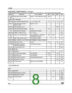
VCM SECTION
CURRENT SENSE AMPLIFIER
Vts
Common mode input voltage
GBD - not tested
-0.6
VM+1
V
range.
Sns _vof
f
Input offset voltage
-12
-5%
-5%
12
mV
Sns_gain0 Differential Voltage GAIN0
Sns _gain1 Differential Voltage GAIN1
Reg09H ‘b7’ = 0
Reg09H ‘b7’ = 1
4.5
16
+5%
+5%
250
Sns_low VSENSE output saturation
Iload=+/-1mA
mV
voltage
Vin_diff=+/- 500mV
Sns_high
4.75
1
V
sns_slew Output slew rate
Sns_band -3dB Bandwidth
Cload=50pF
V/µs
kHz
Guaranteed by design
200
400
sns _cmrr Common mode rejection ratio
f < 10 KHz, tested at DC only
CMRR=A
70
60
dB
dB
V DIFF/AV CM
sns _svrr supply voltage rejection ratio VCV f < 10 KHz, tested at DC only
ERROR SUMMING AMPLIFIER
err _gain Voltage gain
no load
60
dB
MHz
V/µS
µA
err _band Unity gain bandwidth
err _slew Output Slew Rate
err _ibias Input bias current
err _off Input offset voltage
err_svrr supply voltage rejection ratio
Guaranteed by design
Cload=50pF
4
0
1.5
1
-10
60
10
mV
dB
f < 10 KHz, tested at DC only
Isink = 1 mA, referred to Vref25
err _clamp Low output (clamp) voltage
low
TBD
V
7/46

 STMICROELECTRONICS [ ST ]