L6599
Application information
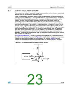
Essentially, RF
will define the switching frequency f
above which the L6599 will enter
max
max
burst-mode operation. Once fixed f
, RF
will be found from the relationship:
max
max
RFmin
3
8
-- --------------------
RFmax
=
⋅
f
--m-----a--x- – 1
fmin
Note that, unlike the f
considered in the previous section ("Chapter 7.1: Oscillator"), here
max
f
is associated to some load Pout greater than the minimum one. Pout will be such that
max
B B
the transformer's peak currents are low enough not to cause audible noise.
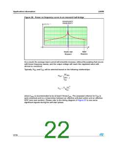
Resonant converter's switching frequency, however, depends also on the input voltage;
hence, in case there is quite a large input voltage range with the circuit of Figure 23 the
value of Pout would change considerably. In this case it is recommended to use the
B
arrangement shown in Figure 24 where the information on the converter's input voltage is
added to the voltage applied to the STBY pin. Due to the strongly non-linear relationship
between switching frequency and input voltage, it is more practical to find empirically the
right amount of correction R / (R + R ) needed to minimize the change of Pout . Just be
A
A
B
B
careful in choosing the total value R + R much greater than R to minimize the effect on
A
B
C
the LINE pin voltage (see Chapter 7.6: Line sensing function).
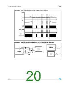
Whichever circuit is in use, its operation can be described as follows. As the load falls below
the value Pout the frequency will try to exceed the maximum programmed value f and
B
max
the voltage on the STBY pin (V
) will go below 1.25V. The IC will then stop with both
STBY
gate-drive outputs low, so that both MOSFETs of the half-bridge leg are in OFF-state. The
voltage V will now increase as a result of the feedback reaction to the energy delivery
STBY
stop and, as it exceeds 1.3V, the IC will restart switching. After a while, V
will go down
STBY
again in response to the energy burst and stop the IC. In this way the converter will work in a
burst-mode fashion with a nearly constant switching frequency. A further load decrease will
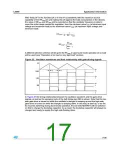
then cause a frequency reduction, which can go down even to few hundred hertz. The timing
diagram of Figure 25 illustrates this kind of operation, showing the most significant signals.
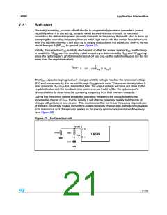
A small capacitor (typically in the hundred pF) from the STBY pin to ground, placed as close
to the IC as possible to reduce switching noise pick-up, will help get clean operation.
To help the designer meet energy saving requirements even in power-factor-corrected
systems, where a PFC pre-regulator precedes the DC-DC converter, the device allows that
the PFC pre-regulator can be turned off during burst-mode operation, hence eliminating the
no-load consumption of this stage (0.5 ÷ 1W). There is no compliance issue in that because
EMC regulations on low-frequency harmonic emissions refer to nominal load, no limit is
envisaged when the converter operates with light or no load.
To do so, the device provides pin 9 (PFC_STOP): it is an open collector output, normally
open, that is asserted low when the IC is idle during burst-mode operation. This signal will
be externally used for switching off the PFC controller and the pre-regulator as shown in
Figure 26 When the L6599 is in UVLO the pin is kept open, to let the PFC controller start
first.
19/36

 STMICROELECTRONICS [ ST ]