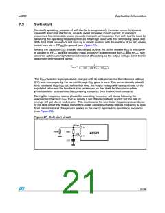
L6599
Application information
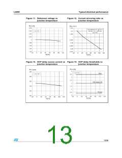
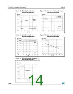
After fixing CF in the hundred pF or in the nF (consistently with the maximum source
capability of the RF pin and trading this off against the total consumption of the device),
min
the value of RF
and RF
will be selected so that the oscillator frequency is able to
min
max
cover the entire range needed for regulation, from the minimum value f
(at minimum input
min
voltage and maximum load) to the maximum value f
minimum load):
(at maximum input voltage and
max
1
RFmin= -----------------------------------
3 ⋅ CF ⋅ fmin
RFmin
RFmax= --------------------
f
--m-----a--x- – 1
fmin
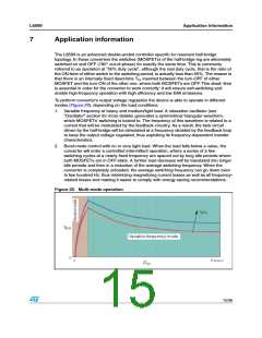
A different selection criterion will be given for RF
in case burst-mode operation at no-load
max
will be used (see "Operation at no load or very light load" section).
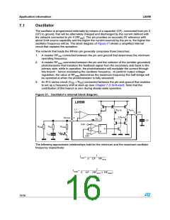
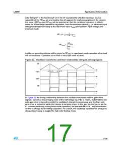
Figure 22. Oscillator waveforms and their relationship with gate-driving signals
CF
TD
TD
t
t
HVG
LVG
HB
t
t
In Figure 22 the timing relationship between the oscillator waveform and the gate-drive
signals, as well as the swinging node of the half-bridge leg (HB) is shown. Note that the low-
side gate-drive is turned on while the oscillator's triangle is ramping up and the high-side
gate-drive is turned on while the triangle is ramping down. In this way, at start-up, or as the
IC resumes switching during burst-mode operation, the low-side MOSFET will be switched
on first to charge the bootstrap capacitor. As a result, the bootstrap capacitor will always be
charged and ready to supply the high-side floating driver.
17/36

 STMICROELECTRONICS [ ST ]