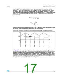
Application information
L6599
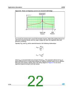
7.2
Operation at no load or very light load
When the resonant half-bridge is lightly loaded or unloaded at all, its switching frequency will
be at its maximum value. To keep the output voltage under control in these conditions and to
avoid losing soft-switching, there must be some significant residual current flowing through
the transformer's magnetizing inductance. This current, however, produces some
associated losses that prevent converter's no-load consumption from achieving very low
values.
To overcome this issue, the L6599 enables the designer to make the converter operate
intermittently (burst-mode operation), with a series of a few switching cycles spaced out by
long idle periods where both MOSFETs are in OFF-state, so that the average switching
frequency can be substantially reduced. As a result, the average value of the residual
magnetizing current and the associated losses will be considerably cut down, thus
facilitating the converter to comply with energy saving recommendations.
The device can be operated in burst-mode by using pin 5 (STBY): if the voltage applied to
this pin falls below 1.25V the IC will enter an idle state where both gate-drive outputs are
low, the oscillator is stopped, the soft-start capacitor C keeps its charge and only the 2V
SS
reference at RF
pin stays alive to minimize IC's consumption and V capacitor's
min
CC
discharge. The IC will resume normal operation as the voltage on the pin exceeds 1.25V by
50mV.
To implement burst-mode operation the voltage applied to the STBY pin needs to be related
to the feedback loop. Figure 23 shows the simplest implementation, suitable with a narrow
input voltage range (e.g. when there is a PFC front-end).
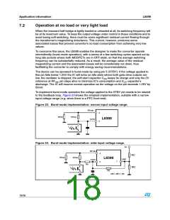
Figure 23. Burst-mode implementation: narrow input voltage range.
RFmin
4
Fmin
R
Fmax
R
Fmin
R
Fmax
R
L6599
STBY
5
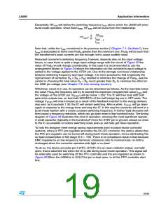
Figure 24. Burst-mode implementation: wide input voltage range.
B+
RFmin
STBY
4
5
D
RRC
Fmin
R
Fmax
R
L6599
LINE
L6599
7
A
R
C
R
RD
B
R
A
R
B
C
+ R >> R
18/36

 STMICROELECTRONICS [ ST ]