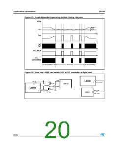
Application information
L6599
7.1
Oscillator
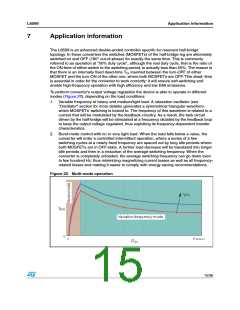
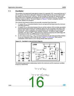
The oscillator is programmed externally by means of a capacitor (CF), connected from pin 3
(CF) to ground, that will be alternately charged and discharged by the current defined with
the network connected to pin 4 (RF ). The pin provides an accurate 2V reference with
min
about 2mA source capability and the higher the current sourced by the pin is, the higher the
oscillator frequency will be. The block diagram of Figure 21 shows a simplified internal
circuit that explains the operation.
The network that loads the RFmin pin generally comprises three branches:
1. A resistor RF
connected between the pin and ground that determines the minimum
min
operating frequency;
2. A resistor RF
connected between the pin and the collector of the (emitter-grounded)
max
phototransistor that transfers the feedback signal from the secondary side back to the
primary side; while in operation, the phototransistor will modulate the current through
this branch - hence modulating the oscillator frequency - to perform output voltage
regulation; the value of RF
determines the maximum frequency the half-bridge will
max
be operated at when the phototransistor is fully saturated;
3. An R-C series circuit (C + R ) connected between the pin and ground that enables
SS
SS
to set up a frequency shift at start-up (see Chapter 7.3: Soft-start). Note that the
contribution of this branch is zero during steady-state operation.
Figure 21. Oscillator's internal block diagram.
L6599
2 V
KM·IR
KM·IR
+
-
3
CF
2·KM·IR
RFmin
4
IR
CF
0.9V
1 V
+
-
S
R
RFmin
RSS
RFmax
Q
+
-
CSS
3.9V
4 V
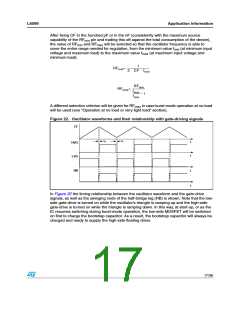
The following approximate relationships hold for the minimum and the maximum oscillator
frequency respectively:
1
f
min= ------------------------------------------
3 ⋅ CF ⋅ RFmin
1
f
max= --------------------------------------------------------------------------
| |
3 ⋅ CF ⋅ (RFmin RFmax
)
16/36

 STMICROELECTRONICS [ ST ]