PDF
最近搜索
热门搜索
发布采购

| 型号: | SST34HF1621-70-4C-LFP |
| PDF下载: | 下载PDF文件 查看货源 |
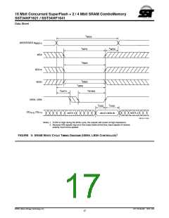
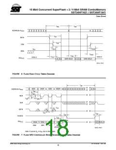
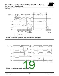
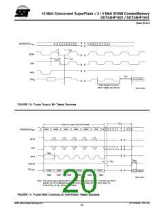
| 内容描述: | 16兆位并行的SuperFlash + 2/4兆位的SRAM ComboMemory [16 Mbit Concurrent SuperFlash + 2 / 4 Mbit SRAM ComboMemory] |
| 分类和应用: | 内存集成电路静态存储器 |
| 文件页数/大小: | 32 页 / 480 K |
| 品牌: |  SST [ SILICON STORAGE TECHNOLOGY, INC ] SST [ SILICON STORAGE TECHNOLOGY, INC ] |
专业IC领域供求交易平台:提供全面的IC Datasheet资料和资讯,Datasheet 1000万数据,IC品牌1000多家。