16 Mbit Concurrent SuperFlash + 2 / 4 Mbit SRAM ComboMemory
SST34HF1621 / SST34HF1641
Data Sheet
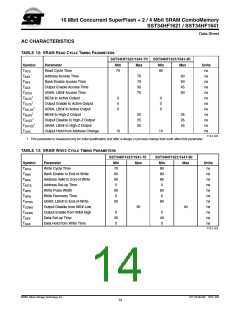
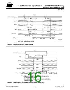
T
RCS
ADDRESSES A
MSS-0
BES1#
BES2
T
T
OHS
AAS
T
BES
T
BES
T
T
BLZS
BHZS
T
OE#
OES
T
T
OLZS
OHZS
T
BYES
UBS#, LBS#
T
T
BYLZS
BYHZS
DQ
15-0
DATA VALID
523 ILL F15.0
A
= Most Significant SRAM Address
MSS
FIGURE 3: SRAM READ CYCLE TIMING DIAGRAM
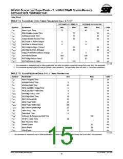
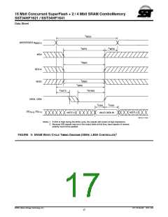
T
WCS
ADDRESSES A
MSS-0
WE#
T
ASTS
T
T
WPS
WRS
T
AWS
T
BWS
BES1#
BES2
T
BWS
T
BYWS
UBS#, LBS#
T
OEWS
T
ODWS
T
T
DHS
DSS
NOTE 2
NOTE 2
VALID DATA IN
DQ
DQ
7-0
15-8,
523 ILL F16.2
Notes: 1. If OE# is High during the Write cycle, the outputs will remain at high impedance.
2. If BES1# goes Low or BES2 goes high coincident with or after WE# goes Low,
the output will remain at high impedance.
If BES1# goes High or BES2 goes low coincident with or before WE# goes High,
the output will remain at high impedance.
Because DIN signals may be in the output state at this time, input signals of reverse
polarity must not be applied.
FIGURE 4: SRAM WRITE CYCLE TIMING DIAGRAM (WE# CONTROLLED)1
©2001 Silicon Storage Technology, Inc.
S71172-05-000 10/01 523
16

 SST [ SILICON STORAGE TECHNOLOGY, INC ]