16 Mbit Concurrent SuperFlash + 2/4/8 Mbit SRAM ComboMemory
SST34HF1602C / SST34HF1622C / SST34HF1642C
SST34HF1642D / SST34HF1682D / SST34HF1622S / SST34HF1642S
Advance Information
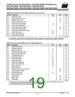
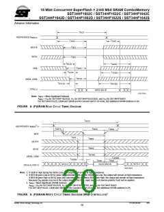
T
RCS
ADDRESSES A
MSS-0
T
T
OHS
AAS
T
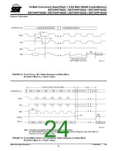
BES1#
BES2
BES
T
BES
T
T
BLZS
BHZS
T
OES
OE#
T
OLZS
T
OHZS
T
BYES
UBS#, LBS#
T
BYLZS
T
BYHZS
DQ
15-0
DATA VALID
1256 F04.0
Note: AMSS = Most Significant Address
MSS = A16 for SST34HF1622C/S, A17 for SST34HF1622C/D/S, and A18 for SST34HF1682D
For SST34HF16x2S, LBS# and UBS# are No Connect and in x8 mode, the additional SRAM address is SA.
A
FIGURE 5: (P)SRAM READ CYCLE TIMING DIAGRAM
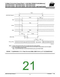
T
WCS
3
ADDRESSES A
MSS -0
T
T
ASTS
T
WPS
WRS
WE#
BES1#
BES2
T
AWS
T
BWS
T
T
BWS
BYWS
UBS#, LBS#
T
OEWS
T
DHS
T
ODWS
T
DSS
VALID DATA IN
NOTE 2
NOTE 2
DQ
DQ
7-0
15-8,
1256 F05.0
Note: 1. If OE# is High during the Write cycle, the outputs will remain at high impedance.
2. If BES1# goes Low or BES2 goes high coincident with or after WE# goes Low, the output will remain at high impedance.
If BES1# goes High or BES2 goes low coincident with or before WE# goes High, the output will remain at high impedance.
Because DIN signals may be in the output state at this time, input signals of reverse polarity must not be applied.
3. AMSS = Most Significant SRAM Address
A
MSS = A16 for SST34HF1622C/S, A17 for SST34HF1622C/D/S, and A18 for SST34HF1682D
For SST34HF16x2S, LBS# and UBS# are No Connect and in x8 mode, the additional SRAM address is SA.
FIGURE 6: (P)SRAM WRITE CYCLE TIMING DIAGRAM (WE# CONTROLLED)1
©2004 Silicon Storage Technology, Inc.
S71256-00-000
3/04
20

 SST [ SILICON STORAGE TECHNOLOGY, INC ]