16 Mbit Concurrent SuperFlash + 2/4/8 Mbit SRAM ComboMemory
SST34HF1602C / SST34HF1622C / SST34HF1642C
SST34HF1642D / SST34HF1682D / SST34HF1622S / SST34HF1642S
Advance Information
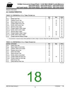
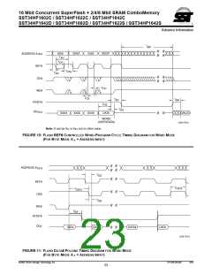
TABLE 14: FLASH READ CYCLE TIMING PARAMETERS VDD = 2.7-3.3V
Symbol Parameter
Min
Max
Units
ns
TRC
TCE
TAA
Read Cycle Time
70
Chip Enable Access Time
Address Access Time
70
70
35
ns
ns
TOE
TCLZ
TOLZ
Output Enable Access Time
BEF# Low to Active Output
OE# Low to Active Output
BEF# High to High-Z Output
OE# High to High-Z Output
Output Hold from Address Change
RST# Pulse Width
ns
1
1
0
0
ns
ns
1
TCHZ
TOHZ
20
20
ns
1
ns
1
TOH
0
ns
1
TRP
500
50
ns
1
TRHR
RST# High Before Read
RST# Pin Low to Read
ns
1,2
TRY
20
µs
T14.0 1256
1. This parameter is measured only for initial qualification and after the design or process change that could affect this parameter.
2. This parameter applies to Sector-Erase, Block-Erase and Program operations. This parameter does not apply to Chip-Erase.
TABLE 15: FLASH PROGRAM/ERASE CYCLE TIMING PARAMETERS
Symbol Parameter
Min
Max
Units
µs
ns
ns
ns
ns
ns
ns
ns
ns
ns
ns
ns
ns
ns
µs
ns
µs
ms
ms
TBP
Word-Program Time
10
TAS
Address Setup Time
Address Hold Time
WE# and BEF# Setup Time
WE# and BEF# Hold Time
OE# High Setup Time
OE# High Hold Time
BEF# Pulse Width
0
40
0
TAH
TCS
TCH
TOES
TOEH
TCP
0
0
10
40
40
30
30
30
0
TWP
TWPH
WE# Pulse Width
1
WE# Pulse Width High
BEF# Pulse Width High
Data Setup Time
1
TCPH
TDS
1
TDH
Data Hold Time
1
TIDA
Software ID Access and Exit Time
Erase-Suspend Latency
RY/BY# Delay Time
Bus# Recovery Time
Sector-Erase
150
20
TES
1,2
TBY
TBR
TSE
TBE
90
1
1
25
25
50
Block-Erase
TSCE
Chip-Erase
ms
T15.0 1256
1. This parameter is measured only for initial qualification and after a design or process change that could affect this parameter.
2. This parameter applies to Sector-Erase, Block-Erase, and Program operations.
This parameter does not apply to Chip-Erase operations.
©2004 Silicon Storage Technology, Inc.
S71256-00-000
3/04
19

 SST [ SILICON STORAGE TECHNOLOGY, INC ]