A d v a n c e I n f o r m a t i o n
Type 1 SRAM
4/8 Megabit CMOS SRAM
Common Features
Process Technology: Full CMOS
Power Supply Voltage: 2.7~3.3V
Three state outputs
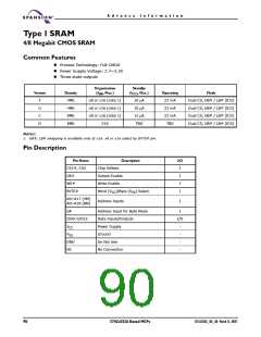
Organization
Standby
Version
Density
4Mb
(ISB1, Max.)
x8 or x16 (note 1)
x8 or x16 (note 1)
x8 or x16 (note 1)
X16
(ICC2, Max.)
Operating
22 mA
22 mA
22 mA
TBD
Mode
F
G
C
D
10 µA
10 µA
15 µA
TBD
Dual CS, UB# / LB# (tCS)
Dual CS, UB# / LB# (tCS)
Dual CS, UB# / LB# (tCS)
Dual CS, UB# / LB# (tCS)
4Mb
8Mb
8Mb
Notes:
1. UB#, LB# swapping is available only at x16. x8 or x16 select by BYTE# pin.
Pin Description
Pin Name
CS1#, CS2
OE#
Description
I/O
Chip Selects
I
I
I
I
Output Enable
WE#
Write Enable
BYTE#
Word (VCC)/Byte (VSS) Select
A0~A17 (4M)
A0~A18 (8M)
Address Inputs
I
SA
Address Input for Byte Mode
Data Inputs/Outputs
Power Supply
I
I/O
-
I/O0~I/O15
VCC
VSS
Ground
-
DNU
Do Not Use
-
NC
No Connection
-
90
S71GL032A Based MCPs
S71GL032A_00_A0 March 31, 2005

 SPANSION [ SPANSION ]