P R E L I M I N A R Y
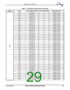
Table 3. Page Select (Continued)
Word 6
Word 7
1
1
1
1
0
1
Simultaneous Read/Write Operation
In addition to the conventional features (read, program, erase-suspend read, and
erase-suspend program), the device is capable of reading data from one bank of
memory while a program or erase operation is in progress in another bank of
memory (simultaneous operation). The bank can be selected by bank addresses
(PL127J: A22–A20, PL129J and PL064J: A21–A19, PL032J: A20–A18) with zero
latency.
The simultaneous operation can execute multi-function mode in the same bank.
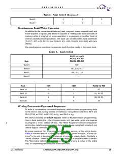
Table 4. Bank Select
PL127J: A22–A20
PL064J: A21–A19
PL032J: A20–A18
Bank
Bank A
Bank B
Bank C
Bank D
000
001, 010, 011
100, 101, 110
111
Bank
CE1#
CE2#
PL129J: A21–A20
00
Bank 1A
Bank 1B
Bank 2A
Bank 2B
0
0
1
1
1
1
0
0
01, 10, 11
00, 01, 10
11
Writing Commands/Command Sequences
To write a command or command sequence (which includes programming data
to the device and erasing sectors of memory), the system must drive WE# and
CE# (CE1# or CE#2 in PL129J) to VIL, and OE# to VIH
.
The device features an Unlock Bypass mode to facilitate faster programming.
Once a bank enters the Unlock Bypass mode, only two write cycles are required
to program a word, instead of four. The “Word Program Command Sequence”
section has details on programming data to the device using both standard and
Unlock Bypass command sequences.
An erase operation can erase one sector, multiple sectors, or the entire device.
Table 4 indicates the set of address space that each sector occupies. A “bank ad-
dress” is the set of address bits required to uniquely select a bank. Similarly, a
“sector address” refers to the address bits required to uniquely select a sector.
The “Command Definitions” section has details on erasing a sector or the entire
chip, or suspending/resuming the erase operation.
April 7, 2005 31107A62
S29PL127J/S29PL129J/S29PL064J/S29PL032J
23

 SPANSION [ SPANSION ]