P R E L I M I N A R Y
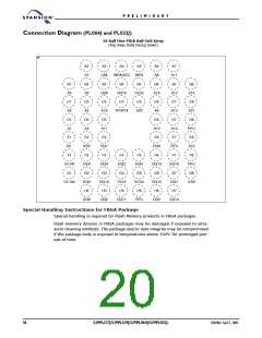
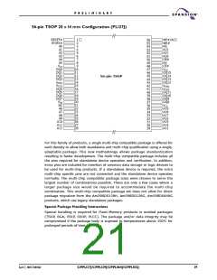
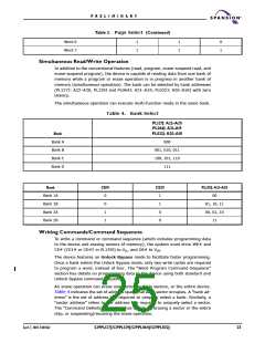
56-pin TSOP 20 x 14 mm Configuration (PL127J)
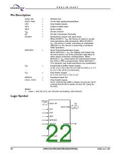
RESET#
RY/BY#
A0
1
2
3
4
5
6
7
8
9
10
11
12
13
14
15
16
17
18
19
20
21
22
23
24
25
26
27
28
WP#/ACC
WE#
NC
A22
A21
A20
OE#
NC
CE#
VSS
DQ15
DQ14
DQ13
DQ12
VSSQ
VCCQ
DQ11
DQ10
DQ9
DQ8
VCC
56
55
54
53
52
51
50
49
48
47
46
45
44
43
42
41
40
39
38
37
36
35
34
33
32
31
30
29
A1
A2
A3
A4
A5
VCC
DQ0
DQ1
DQ2
DQ3
VSSQ
VCCQ
DQ4
DQ5
DQ6
DQ7
VSS
NC
56-pin TSOP
A6
A7
A8
A9
A10
A11
A12
A19
A18
A17
A16
A15
A14
A13
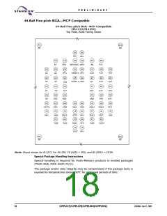
For this family of products, a single multi-chip compatible package is offered for
each density to allow both standalone and multi-chip qualification using a single,
adaptable package. This new methodology allows package standardization
resulting in faster development. The multi-chip compatible package includes all
the pins required for standalone device operation and verification. In addition,
extra pins are included for insertion of common data storage or logic devices to
be used for multi-chip products. If a standalone device is required, the extra
multi-chip specific pins are not connected and the standalone device operates
normally. The multi-chip compatible package sizes were chosen to serve the
largest number of combinations possible. There are only a few cases where a
larger package size would be required to accommodate the multi-chip
combination. This multi-chip compatible package set does not allow for direct
package migration from the Am29BDS128H, Am29BDS128G, Am29BDS640G
products, which use legacy standalone packages.
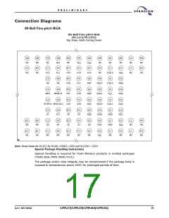
Special Package Handling Instructions
Special handling is required for Flash Memory products in molded packages
(TSOP, BGA, PDIP, SSOP, PLCC). The package and/or data integrity may be
compromised if the package body is exposed to temperatures above 150°C for
prolonged periods of time.
April 7, 2005 31107A62
S29PL127J/S29PL129J/S29PL064J/S29PL032J
19

 SPANSION [ SPANSION ]