P R E L I M I N A R Y
Requirements for Reading Array Data
To read array data from the outputs, the system must drive the OE# and appro-
priate CE# pins (For PL129J - CE1#/CE2# pins) to VIL. In PL129J, CE1# and
CE2# are the power control and select the lower (CE1#) or upper (CE2#) halves
of the device. CE# is the power control. OE# is the output control and gates array
data to the output pins. WE# should remain at VIH
.
The internal state machine is set for reading array data upon device power-up,
or after a hardware reset. This ensures that no spurious alteration of the memory
content occurs during the power transition. No command is necessary in this
mode to obtain array data. Standard microprocessor read cycles that assert valid
addresses on the device address inputs produce valid data on the device data
outputs. Each bank remains enabled for read access until the command register
contents are altered.
Refer to Table 33 for timing specifications and to Figure 11 for the timing diagram.
ICC1 in the DC Characteristics table represents the active current specification for
reading array data.
Random Read (Non-Page Read)
Address access time (tACC) is equal to the delay from stable addresses to valid
output data. The chip enable access time (tCE) is the delay from the stable ad-
dresses and stable CE# to valid data at the output inputs. The output enable
access time is the delay from the falling edge of the OE# to valid data at the out-
put inputs (assuming the addresses have been stable for at least tACC–tOE time).
Page Mode Read
The device is capable of fast page mode read and is compatible with the page
mode Mask ROM read operation. This mode provides faster read access speed for
random locations within a page. Address bits Amax–A3 select an 8 word page,
and address bits A2–A0 select a specific word within that page. This is an asyn-
chronous operation with the microprocessor supplying the specific word location.
The random or initial page access is tACC or tCE and subsequent page read ac-
cesses (as long as the locations specified by the microprocessor falls within that
page) is equivalent to tPACC. When CE# (CE1# and CE#2 in PL129J) is deasserted
(=VIH), the reassertion of CE# (CE1# or CE#2 in PL129J) for subsequent access
has access time of tACC or tCE. Here again, CE# (CE1# /CE#2 in PL129J)selects
the device and OE# is the output control and should be used to gate data to the
output inputs if the device is selected. Fast page mode accesses are obtained by
keeping Amax–A3 constant and changing A2–A0 to select the specific word within
that page.
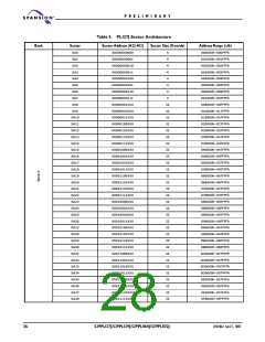
Table 3. Page Select
Word
A2
0
A1
0
A0
0
Word 0
Word 1
Word 2
Word 3
Word 4
Word 5
0
0
1
0
1
0
0
1
1
1
0
0
1
0
1
22
S29PL127J/S29PL129J/S29PL064J/S29PL032J
31107A62 April 7, 2005

 SPANSION [ SPANSION ]