P R E L I M I N A R Y
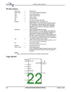
Device Bus Operations
This section describes the requirements and use of the device bus operations,
which are initiated through the internal command register. The command register
itself does not occupy any addressable memory location. The register is a latch
used to store the commands, along with the address and data information
needed to execute the command. The contents of the register serve as inputs to
the internal state machine. The state machine outputs dictate the function of the
device. Table 1 lists the device bus operations, the inputs and control levels they
require, and the resulting output. The following subsections describe each of
these operations in further detail.
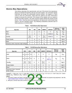
Table 1. PL127J Device Bus Operations
Addresses
(Amax–A0)
DQ15–
DQ0
Operation
CE#
L
OE#
L
WE#
RESET#
WP#/ACC
X
Read
Write
H
L
H
H
AIN
AIN
DOUT
DIN
L
H
X (Note 2)
VIO
0.3 V
±
VIO ±
0.3 V
Standby
X
X
X (Note 2)
X
High-Z
Output Disable
Reset
L
X
X
H
X
X
H
X
X
H
X
X
X
X
X
High-Z
High-Z
DIN
L
Temporary Sector Unprotect (High Voltage)
VID
AIN
Table 2. PL129J Device Bus Operations
Addresses
(A21–A0)
DQ15–
DQ0
Operation
CE1#
CE2#
OE#
WE#
RESET#
WP#/ACC
L
H
L
H
L
Read
L
H
H
X
AIN
DOUT
H
L
X
Write
H
X
L
H
AIN
X
DIN
(Note 2)
H
VIO
0.3 V
±
VIO
0.3 V
±
VIO ±
0.3 V
Standby
X
X
High-Z
Output Disable
Reset
L
L
H
X
H
X
H
L
X
X
X
X
High-Z
High-Z
X
X
Temporary Sector Unprotect
(High Voltage)
X
X
X
X
VID
X
AIN
DIN
Legend: L = Logic Low = VIL, H = Logic High = VIH, VID = 11.5–12.5 V, VHH = 8.5–9.5 V, X = Don’t Care, SA = Sector
Address, AIN = Address In, DIN = Data In, DOUT = Data Out
Notes:
1. The sector protect and sector unprotect functions may also be implemented via programming equipment. See the
"High Voltage Sector Protection" section section.
2. WP#/ACC must be high when writing to upper two and lower two sectors.
April 7, 2005 31107A62
S29PL127J/S29PL129J/S29PL064J/S29PL032J
21

 SPANSION [ SPANSION ]